There are several types of field programmable gate arrays (FPGAs) available in the market today. Each of these FPGAs offers different functions and capabilities. The programmable fabric is the core of any FPGA. Also, this programmable fabric is an array of logic elements also known as programmable logic blocks.
The FPGA fabric also comprises other elements like block RAM, digital signal processing, phase lock loops, clock managers, and serializer/deserializer blocks. Different FPGAs provide a wide range of features, capacities, and functions targeted at various applications and markets.
There is a wide array of FPGA vendors like Altera, Efinix, and Xilinx among others. However, the programmable devices offered by Xilinx ranges from modest to extremely high. This company addresses various market segments and offers a wide variety of deployment methods.
What is Xilinx FPGA?
Xilinx (field programmable gate array) FPGA is a development board use to perform logical operations. This board comprises an integrated network of logic blocks. Also, it comprises individual configurable logic blocks connected via programmable interconnects. The Xilinx FPGA can be programmed when integrated in the field unlike ASICs.
Application Specific Integrated Circuit (ASIC) is primarily design to carry out a certain task. Therefore, it can only carry out that particular function you can’t modify it to something else. On the other hand, you can reprogram and reuse an FPGA. Also, FPGA board is more flexible as regards personalization and customization. Therefore, Xilinx FPGA board is highly preferred to an ASIC in some particular applications.
Xilinx is an American-based technology company that specializes in the production and supply of programmable logic devices. Also, this company invented the first viable FPGA. Xilinx FPGA allows designers and engineers to prioritize product functions and features and as well reconfigure hardware for particular projects and application after installing them in the field. This is the reason behind the term field programmable. Also, the gate arrays refer to two dimensional arrays.
Xilinx offers a wide range of FPGA development and evaluation boards. Designers can choose a low-cost FPGA integrated at an earlier technology node based on the target applications. For instance, you can select a high bandwidth, high capacity, and high performance device integrated at the latest technology node and design tools.
Xilinx produces a vast range of FPGA boards. Also, Xilinx FPGAs are widely used across a wide variety of applications. For instance, Versal devices are mainly optimized for artificial learning and computer-intensive applications. Also, VHDL is a programmable language for FPGAs. VHDL means very hardware description language.
How Does Xilinx FPGA Work?
FPGAs allow you to reconfigure them and start acting like the desired circuit. Also, you can reconfigure an FPGA board over and over again. FPGA configuration is RAM based and as such, it allows unlimited reconfiguration. FPGAs can only create digital circuits. VHDL which means Very Hardware Description Language is the programming language used for FPGA boards.
The VHDL programs the Xilinx FPGA board to carry out different functions. VHDL is a programming language that describes digital and mixed-signal systems like FPGAs. Also, VHDL is a dataflow language. Xilinx FPGA contains configurable blocks interconnected through software programs. With these programs, designers can link different blocks by interchanging logic controls. Xilinx FPGA offers a large amount of.
Benefits of Xilinx FPGA
Efficiency
Xilinx FPGA is more efficient as regards their process time. Also, Xilinx FPGA boards provide very tight timing. These boards comprise offload functions and acceleration capabilities for CPU. Furthermore, they help to enhance the performance of your system. FPGA boards are crucial for performing parallel execution. These boards are very efficient as they can regulate several channels.
Ease of use
This is one of the benefits you will enjoy when you use Xilinx FPGA boards. Also, Xilinx FPGA boards are user friendly. Therefore, they are a great option for beginners. Some FPGA development boards can be very complex.
Flexibility
These FPGAs allow you to add custom digital circuits to any design. Also, these FPGA boards offer a flexible reconfigurable computing capability. Therefore, this allows users to reprogram the device. Also, Xilinx FPGAs offers cost-optimized solutions.
Security
There is low risk of malicious modifications when programming. Also, this board offers various security solutions to users and analog devices.
Programmability
These FPGAs are reprogrammable. This means that you can reprogram them many times even after you have designed and implemented the circuits. Also, Xilinx FPGA boards allow you to modify, update, and change their functionality to execute a different task. Furthermore, the ability to reprogram these boards reduces the cost and effort needed for maintaining them. You can just update their codes and program them with new functionality.
Real-time application
Xilinx FPGAs are suitable for real time applications. Also, these boards offer more process within a very short time.
Types of Xilinx FPGA Family

Xilinx FPGA 3000 series
Xilinx FPGA 3000 series features high-density digital integrated circuits. This FPGA series’s user-programmable array architecture comprises a configuration program store and different types of configurable elements. The configurable elements include a core array of Configurable Logic Blocks (CLBs), resources for interconnection, and Input/output blocks. Analog devices
I Xilinx 3000 field programmable arrays offer various package styles, speed grades, logic capacities, and temperature ranges. Xilinx FPGA 3000 series comprises four different family groups. These include XC3100L family, XC3000A family, XC3100A family, and XC3000L family. Also, these families have a similar architecture, design and programming methodology, package pin-outs, and development software.
- XC3000A family is an improved version of the XC3000 family. Also, it offers user-friendly improvements and more interconnect resources.
- XC3000L family has similar features and architecture with XC3000A family. However, it functions at a supply voltage of 3.3V. This field programmable gate array is ideal for low-power and battery-operated applications.
- XC3100A family is a field programmable gate array similar to XC3000A. Both families are footprint and bitstream compatible. However, XC3100A has improved in-system performance of more than 80 MHz and more toggle rates. Also, this Xilinx FPGA features an additional array size.
- XC3100L family shares similar features and architectures with XC3100A family. However, it functions at a supply voltage of 3.3V.
Xilinx Artix 7
Xilinx Artix 7 FPGA board offers cost-effective performance in areas like signal processing, memory interfaces, and logic among others. This FPGA comprises a compact packaging and footprint. Also, Xilinx Artix 7 FPGA is a good board that comprises 1,066Mb/s DDR3 support and MicroBlaze soft processor. This Xilinx FPGA family offers the lowest power, most optimized and highest performance transceivers.
It is a good FPGA board for cost-sensitive applications that require high-end capabilities. Also, this Xilinx FPGA board offers advanced and integrated AMS technology. Xilinx Artix 7 helps in analog-to-digital conversion. Also, Xilinx Artix 7 includes global routing networks, logic blocks, block RAM and DSP slices.
Xilinx Artix 7 FPGA board has about 215000 LCs. Also, this FPGA offers improved system performance due to the presence of 13Mb block RAM, about 16xg.6G GTs, and 930 GMAC/s 1.2 GB/s LVDS. Xilinx Artix 7 comes in a BGA packaging. Also, Artix 7 has an evaluation board. The evaluation board offers good hardware platform for evaluating and developing Artix 7 FPGAs.
Xilinx Artix 7 FPGA series comprises several families. Some of these families include:
- XC7A100T is a family of Xilinx Artix 7. This family offers high performance per-watt fabric line rates. Also, XC7A100T FPGA comprises machine-vision cameras and low-end wireless backhaul.
- Artix 7100T serves as a development base for Artix 7 FPGAs. Also, this board can become an adaptable tool when considering expansion headers. Furthermore, Artix 7100T comprises MicroBlaze soft processing system.
Xilinx Virtex II
This FPGA series is specifically designed to enhance the configuration of electronic devices. Also, this FPGA integrates the 150 MHz to offer about 102 D-MIPS. This speed can enhance configuration and design of complex FPGA systems.
The Xilinx Virtex II pro is an improved version of Xilinx Virtex II. Also, this version was majorly launched to allow faster system prototyping of different applications. This FPGA development board comprises multi-gigabit serial transceivers and embedded PowerPC processors at no additional charge. Also, this FPGA board offers enhanced DSP processing, performance, memory, and density.
The Xilinx Virtex II offers solution to one of FPGA design problems which is delay in configuration. This FPGA board enables both audio and video systems. Therefore, this helps digital designers in completing designs within a very short time. Furthermore, the Xilinx Virtex II allows flexible signaling of audio and video stream.
The stereo line level outputs and inputs offer support to audio signals. On the other hand, the video integrates PAL/NTSC video recorder in supporting the production of real-time video. Virtex II features enhanced speed architecture which enables fast configurations of the targeted applications and devices. Also, Xilinx Virtex II was primarily designed to create prototypes of multimedia devices.
Xilinx Zynq
Xilinx ZYnq FPGA series comprises integrated features and capabilities. Also, these FPGA boards are ideal for high-performance applications. They address requirements for high-end embedded systems applications like factory automation and video surveillance. Furthermore, the architecture of Xilinx Zynq is different from previous embedded processors and programmable logic.
This FPGA integrates a processor-centric model. Also, Zynq -700 comprises ARM Cortex-A9 MPCore-processor. It integrates the hardware programmability of a field programmable gate array and the software programmability of an ARM-based processor.
Xilinx Zynq device offers system level performance, thanks to its optimized architecture. Also, Zynq device allows differentiated designs for various embedded applications such as camera drivers assistance systems.
Xilinx FPGA Architecture
The Xilinx FPGA architecture comprises several elements.
Configuration Memory of Xilinx FPGA
Xilinx FPGA board comprises a configuration memory. The static memory cell in this memory is specifically designed for noise immunity and high reliability. Even under adverse conditions, the device configuration memory guarantees integrity. The memory cell comprises two CMOS inverters and a pass transistor. You can only write the cell during configuration and then read it at readback.
In addition, the cell offers continuous control during normal operation. Also, the pass transistor is usually off and doesn’t have any effect on cell stability. Analog devices
Input/Output Block
Every IOB offers an interface between the internal user logic and external package pin of the device. Also, every IOB comprises direct input paths and registered paths. Every IOB offers a 3-state output buffer which a direct output signal may drive. With the configuration options, every IOB can have an inversion and a high impedance pull up.
Furthermore, each input circuit features input clamping diodes. This offers electrostatic shielding and helps circuits to posses latch-up generated by input currents. Also, each I/O block comprises output and input storage elements and options chosen by configuration memory cells. Each IOB has an input-buffer option that offers the detection of threshold to translate external signals to internal logic levels.
You can program the global input-buffer threshold to be compatible with CMOS or TTL levels. Also, the buffered input signal may be configured as a latch or flip-flop. The transition times of inputs should be less than 100 ns to achieve reliable operation. Also, the input should not float. Floating input-pin circuits can generate oscillations. Furthermore, there can be more system noise and additional power dissipation.
Each user input/output block comprises a pull-up resistor selected by the program to offer a constant High. The field programmable gate array offers circuitry to prevent any form of electrostatic discharge. Therefore, it is crucial to observe CMOS handling precautions.
In addition, flip-flop delays for input/output block are usually short and as such offering great performance in data and asynchronous clock conditions. IOB buffers must be compatible with CMOS. Also, the network driving Input/output pin becomes the direct data source.
Configurable Logic Block
Configuration logic blocks offer functional elements. These logic blocks are usually arranged within the perimeter of input/output blocks. For instance, the XC3020A comprises 64 blocks in 8 columns and 8 rows. Also, the development system compiles the configuration memory to specify the interconnection and operation of every block. Automatic translation can perform user definition of CLBs.
Every configurable logic block features a combinatorial logic section, internal control section, and two flip flops. Furthermore, there are five different logic units, an enable clock, and an asynchronous direct RESET input, a common clock input. The interconnect elements adjacent to the blocks may drive all units and clocks. Also, every CLB features two outputs which are X and Y. This may trigger interconnect networks.
The combinatorial logic features F or G outputs which supply data input for any flip-flop within a CLB. The two flip-flops in every CLB have similar asynchronous RD.
Flexible routing enables individual or common CLB clocking. The CLB has a combinatorial logic portion which integrates a 32 by 1 look-up table (LUT) to incorporate Boolean functions. Also, variables chosen from two internal block and five logic inputs serve as table address inputs.
Types of Resources for Different Network Interconnect Requirements
Programmable interconnection resources in Xilinx FPGA board offer routing paths to link outputs and inputs of CLB and I/O blocks into logic networks. Also, interconnections that occur between blocks usually comprise a grid of metal segments. The development system offers routing of these interconnections. Basically, there are three different kinds of metal resources that accommodate different network interconnect requirements. These include:
- Direct connection
- General purpose interconnect
- Longlines
General purpose interconnect
General purpose interconnect features a grid of five vertical metal sections and five horizontal metal sections between columns and rows of IOBs and logic. Furthermore, every section is the width or height of a logic block. You can use switching matrices to join the ends of these sections and enable programmed interconnection between the metal sections of rows and columns. Analog devices
Automatic routing may help establish the connections via the switch matrix. Alternatively, you can choose pairs of matrix pins you need to disconnect or connect. Also, the general interconnect areas have special buffers which offer signal isolation for enhanced performance of lengthy nets. Furthermore, the interconnect buffers enable signal propagation in any direction on a particular general interconnect section.
Direct interconnect
This interconnect offers great networks implementation between adjacent IOBs or CLBs. Signal could posses low interconnect propagation when you use the direct interconnect to route signals from one block to another. For every CLB on an FPGA board, it is important to connect the X output directly to the CLB’s B input to its right and then the C input to its left.
Furthermore, the D input block can be driven by direct interconnect above. Direct interconnect can help to improve the speed of high-performance parts of logic. Direct connect is alternate to the I/O block inputs wherever logic blocks become adjacent to IOBs.
Longlines
The longlines are mainly intended for signals that need to travel a long distance. There are three vertical longlines on each interconnection column and there are two horizontal longlines on each interconnection row. An Input/output block or a logic block can drive longlines. This helps to offer a clock line or low skew control within every column of logic blocks. You can program longlines as connectable half-length lines.
Applications of Xilinx FPGA Board
Xilinx FPGA boards are suitable for various markets due to their programmable nature. Also, Xilinx offers a good FPGA board that provides extensive solutions that comprises advanced software, FPGA devices, and simple IP cores.
Aerospace and defense
Xilinx has been providing cutting edge solutions for the development of aerospace and defense devices. FPGA boards play a crucial role in radar systems integrated in electronic intelligence systems. Due to the programmability nature of these FPGAs, these boards are ideal for use in radar imaging and high-resolution optical data processing.
Medical application
Xilinx FPGA board serves monitoring and diagnostic functions in the medical field. Also, these boards help medical equipment to process data. They are available in CT scan, patient monitoring systems, and MRI. Furthermore, these FPGAs comprise high speed serial transceivers which make them ideal for fast interfaces.
Telecommunication application
FPGA boards offer great functions in wireless and wired communications. Also, these boards are ideal for use in backplanes for wired communications. In wireless communications, Xilinx FPGA boards offer great function in cellular base stations. Also, Xilinx FPGAs offer networking solutions and as well address HSPDA, WiMAX, and 5G/6G standards.
Automotive application
The LiDAR system, known as, light detection and ranging needs great sensing abilities. Also, LiDAR has sensing abilities needed for path planning, control, and perception. Xilinx FPGAs help the LiDAR system to perform all these functions.
Server application
Xilinx FPGA board is very crucial in data/servers center. The demand for data process speed keeps rising every day. Therefore, it is crucial to achieve real-time data process in a short time. Also, to achieve better results, there is a need for new functionalities like data analytics and metadata. An FPGA board has the greatest density as regards BRAM.
Types of Xilinx FPGAs Based on Applications
Generally, there are three classifications of FPGAs based on applications. This includes high-end, mid-range, and low-end field programmable gate arrays.
Low end
Low end FPGAs offer low logic density, low complexity per chip, and low power consumption. The Spartan family is a good example of low end field programmable gate arrays.
Mid range
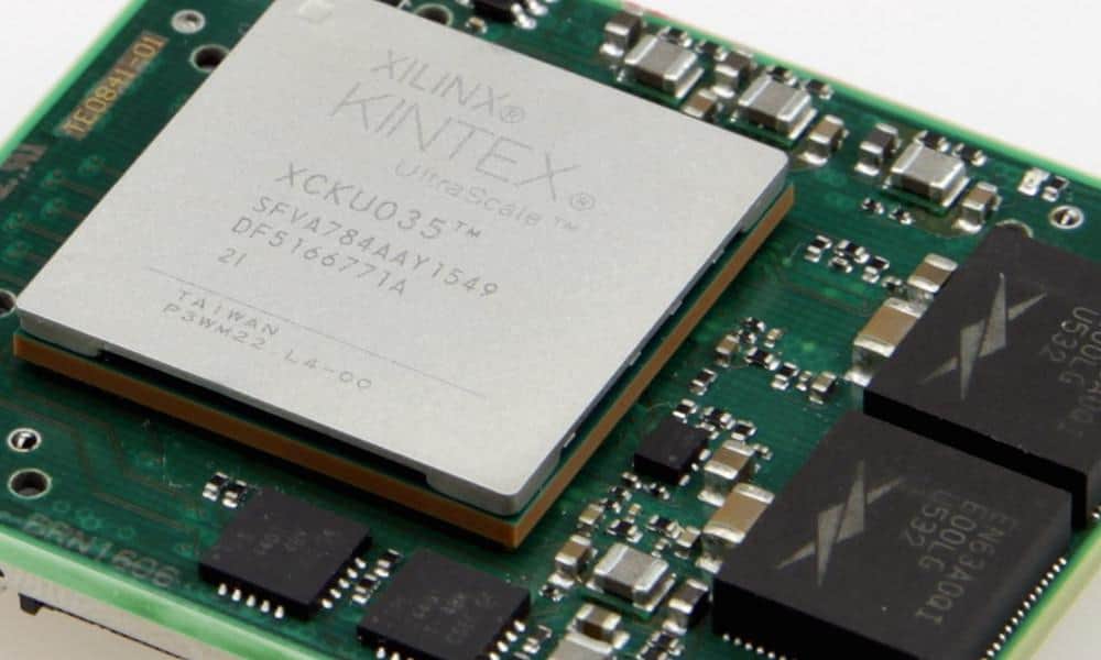
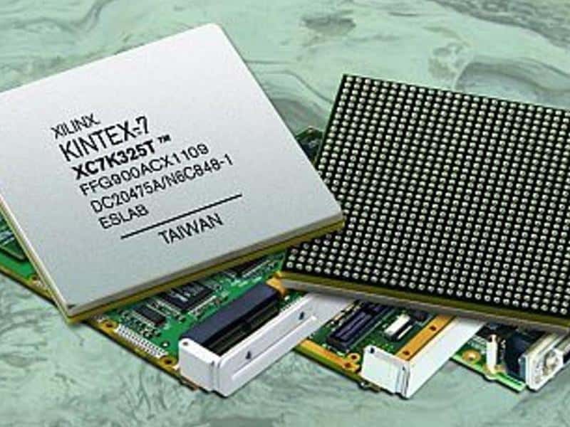
Mid range FPGAs provide optimum solution between high end FPGAs and low end FPGAs. Also, this category of FPGA is offer a balance between cost and performance. The Kintex 7 and Artix 7 series are examples of mid range FPGAs.
High end
High end FPGAs are mainly designed for high performance and logic density. Also, these FPGAs feature enhanced speed architecture which enables fast configurations of the targeted applications and devices. There are great design tools. The Virtex family is a good example of high end FPGAs. System on modules
Conclusion
Xilinx FPGAs are an ideal choice for time critical systems since they have a better processing architecture. Also, Xilinx has a comprehensive multi-node portfolio in the FPGA industry. These FPGAs comprise various elements. These elements are crucial for the performance of Xilinx FPGAs. Xilinx offers a wide range of FPGAs suitable for various applications.
