Have you ever pondered the possible profits from X-raying your PCBs?
X-ray quality inspection and control provide various advantages to the producer and the inspector alike.
The most significant benefits are the great precision of the outcome. And the unveiling of previously hidden characteristics. However, many advantages still remain to guarantee the highest quality PCB getting manufactured.
In this article, we’ll look more closely at the advantages of PCBs and the X-ray technique for detecting PCB flaws. If you feel up to it, then let’s get started.
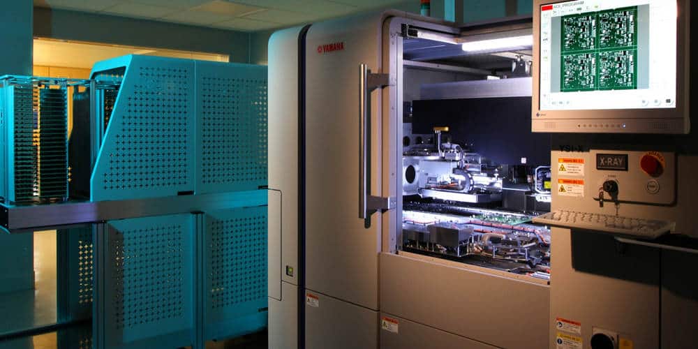
What is an X-Ray PCB Inspection?
In some cases, we may use the term “Automated X-ray Inspection” (AXI). This is a unique type of ray that emits strong EM waves on incredibly short wavelengths. Having a wavelength of fewer than ten nanometers, it is extremely short compared to visible light.
X-rays’ strong penetrating strength is what makes them useful in an industrial context. X-rays have the ability to see through materials that regular light cannot.
How Does X-Ray PCB Inspection Work?
X-rays are commonly used in the manufacturing sector to examine the PCB and its components for flaws. It is useful for figuring out how well something works and finding problems with the design. This takes place throughout the first phases of production and quality control.
The designer places the part to get tested or inspected in between the detection part and the X-ray machine during inspection or testing. X-rays’ ability to penetrate gets affected by things like:
- Radiation produced by an x-ray
- Its density
- What is the nuclear charge of the material?
An X-ray device’s settings can get adjusted beforehand to take all of that into account during the actual inspection. Therefore, the detecting part will reveal a visible part of the filming part. It doesn’t matter if the film is digital or analog; either will do.
Benefits of X-Ray PCB Inspection
1. Allow to inspect of blind vias
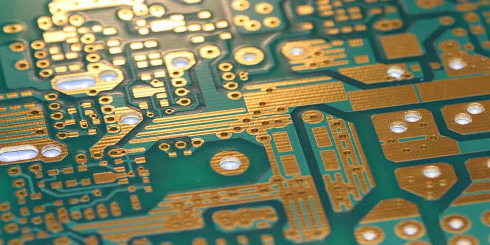
Vias are a crucial part of PCBs because they provide connections between the various board layers.
Although different vias, such as buried vias and blind vias, are utilized to link the boards, they all serve the same purpose.
It is difficult for the quality inspector to determine whether or not these vias are intact simply by looking at them.
Fortunately, PCB X-ray devices emit radiations that may easily pierce through concealed and inaccessible areas, allowing the inspector a clear view of the board’s components and connections.
2. Benefit to check mistakes in landing patterns

Landing patterns of particular parts on the board are a common source of error during PCB Assembly, the process of soldering and mounting components on circuit boards.
The difficulty of having the landing patterns wrong increases if the elements to be put on the electronic board is not among the components provided in the library of frequently used SMD elements.
Often, the design engineer will need to draw up a diagram of the new component’s pinout and its intended placement on the board.
When this diagram is absent, it may be difficult to tell if there is a problem with the landing pattern.
PCB X-ray machines, on the other hand, make it quite simple to evaluate a component’s incorrect landing pattern after it has been mounted on the board.
3. Allow to see through BGAs
BGA is a method for arranging components that allow for the use of extremely small components and the miniaturization of electronic devices.
The use of BGA in quality control and assurance situations is not without its limitations. Components using the BGA technology are typically fitted with little to no gap between them on the board.
As a result of the compact layout, any flaws between the board and its components are invisible to the naked eye of an inspector.
X-rays from PCB X-ray equipment can see through the BGA assembly to evaluate the condition of the parts and the board’s connection.
The images produced by the board X-ray machine allow the inspector to examine individual parts and locate defects without destroying the board.
4. Recognize the false positions of the decoupling capacitors
Decoupling capacitors, which help eliminate transients and oscillations from power supplies, are a common component of virtually every electronic equipment.
These capacitors always have a parallel connection to the power source. They are also located as close as possible to the parts that are in close interaction with the power source.
Yet, if these capacitors are installed incorrectly, the equipment may work poorly or even explode, posing a safety risk to the user.
Visually inspecting a PCB for a bad connection could be challenging due to the near proximity of the many electronic components.
With the help of PCB X-ray equipment, an inspector may spot incorrect component placements and ensure they are fixed prior to releasing the item for sale.
5. Permits Inspectors to catch solder voids
The components are attached to the PCB through soldering. Soldering mistakes can lead to connection failure and poor product quality.
The product also runs the danger of underperforming expectations and perhaps being harmful to the user.
Solder voids, which could result in subpar connections, are inspected in order to head off such problems.
Furthermore, because of the dense packing of BGAs during installation, visual examination of the soldering becomes extremely challenging.
X-ray machines for printed circuit boards (PCBs) are frequently used as a means of overcoming this difficulty, as they allow inspectors to spot solder gaps that could otherwise result in a subpar connection or end product.
6. Easy to determine pin-hole fills
Through-hole connections are used on PCBs, particularly for elements that require a more secure connection when stacked.
In spite of its convenience, this type of connection is prone to flaws such as pin-hole fills. A common cause of this problem is the release of gas during the soldering process.
If the soldering process is carried out at too high a temperature, water vapor will constantly escape, resulting in pin-hole fills.
Visual examination and other insufficient modes of inspection make it difficult to detect these irregularities.
PCB X-ray devices, however, provide the most reliable and precise method of detecting pin-hole fillings during quality assurance testing. Thereby ensuring that the soldering process has not compromised the board in any way.
Conclusion
As you can see, there are several advantages to using X-ray equipment for PCB quality monitoring in the production process.
The expense of failure is another factor to think about, as it can be rather high if the value of your items is not up to par.
Using an X-ray machine for printed circuit boards (PCBs) in quality control helps save the expense of product recalls and malfunctions after it has already been sold.
