In this article, we will be discussing what BGA Assembly means. There are new technologies and techniques coming in different engineering fields as well as engineering-related devices. The use and requirements of integrated circuits with less size is on the rise. This makes the product cost effective and more reliable. To achieve this small size, as well as very dense packaging, you need to use less expensive creation techniques and BGA happens to be one of them.
With the continuous progress and development of electronic technology, all electronic products have started developing towards thinness, lightweight trends, advanced functions, and miniaturization. After upgrading for generations, technologies of chip packaging have resulted in a ratio between the package and chip area to be 1, where the ball grid array (BGA) is now a packaging technology of high density, which has entered into the pragmatic phase.
In BGA surface mount technology, some critical aspects include guaranteeing the reliability of the quality of your BGA soldering, ways of inspecting the BGA’s quality, ways of implementing rework on ball grid arrays having defects. Manufacturers have to be fully aware of all their resolutions. You will understand all these after reading the article.
What is BGA Packaging Technology?
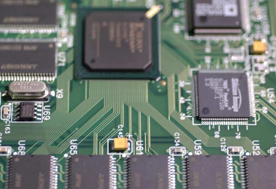
The BGA package has many bumps with ball shape found at the upper surface or the bottom of the tube. Interconnection is possible between the base and body of the package due to these bumps.
BGA, being a packaging technology, features short leads and large lead space through the distribution of I/O ends, which function as columns or balls at the package’s bottom. Based on the different materials for packaging, you can classify BGA components into plastic BGA (PBGA), tape BGA (TBGA), chip-scale package (CSP), ceramic column BGA (CCBGA), and ceramic BGA (CBGA).
Drawing comparisons with quad flat package (QFP) components, you can find the following properties in BGA components.
- Very large I/O end spacing, of which BGA can hold I/O ends with a higher number.
- Reliability of higher packaging, defects of lower soldering, as well as more solid joints for soldering.
- You will also find large spacing in BGA chips between the soldering joints. This makes things easy for soldering and alignment as a result of the alignment amplification system.
- The soldering coplanarity of BGA is sure as the solder compensates automatically for planarity error between the PCB and the chip after melting.
- Offer great electrical and frequency characteristics. This is due to its low mutual inductance and self-inductance, as well as smaller soldering joints.
- It can handle tension and self-alignment automatically between the soldering joints. This results in a great self-centering effect, which causes high reliability.
The main disadvantage has to do with their rework and inspection, which are usually difficult to carry out.
What is BGA Assembly?
BGA SMT has a close relationship with components, solder bga paste, silkscreen, PCB, and soldering. Out of all these, the hardest to handle when performing the process of reflow soldering are the soldering items.
The main element that affects reflow soldering has to do with the setting of the temperature curve. One main method is opening a hole at the middle of BGA at a specific position of a pad. This is at the PCB’s back side. Next is the leading of the thermocouple probe via the hole from underneath the PCB board, stucking it to the pad’s backside and fixing it with a tape with high temperature.
Following is the curve tester of the reflow soldering temperature. This comes with well set parameters, which are properly placed in the oven along with the probe and tray. After comparison and then analysis, you will obtain a temperature curve.
There are four main phases in the reflow temperature curve:
- Preheating
- Heat preservation
- Reflow
The temperature cure and the heating process should ensure that the package reaches reflow temperature. It also ensures that it returns to the pad after the melting of the solder balls with the intermetallic compound, which the pad generates.
With inconsistent heating, packages will unevenly incline towards or fall to one side or the corner of your reflow soldering. This causes inadequate soldering and non-coplanarity.
The aspects below must be properly emphasized regarding BGA soldering.
Prebaking
Normally, plastic packaging absorbs humidity. Heating a chip instantly after it has absorbed humidity present in air, means moisture diffusion will result in cavities present in the chip. Due to this reason, generally, the condition for baking plastic packages must be below 100°C for about six to eight hours.
Oxidation
Before applying them, make sure you inspect all BGA components must be inspected properly to make sure that their pins are properly cleaned and pass through no oxidation.
What are the Types of BGA?

BGA comes in three major types. Let’s consider them in detail.
PBGA
For this BGA category, lamination is useful. This is because the board comes with a plastic packaging and a substrate. Furthermore, you can clearly see the distribution of the solder balls in the lead-free and lead solder.
TBGA
TGBA features a structure that has a cavity. In general, there are two major categories that exist between the chip and substrate. Solder bonding is the first, while lead bonding is the second one.
CBGA
In contrast to other categories, the use of CBGA is much older. The substrate material features multilayer ceramic. The placing of the metallic coating is at the substrate via the use of packaging solder to offer some protection to the pads, leads, and board.
Inspection Method of BGA
BGA Inspection Method and Defects
Once you are through with soldering, the components of the BGA can suffer from some defects. This may be due to assembly equipment, components, as well as soldering and environment technologies. Well-known defects of BGA are loose soldering, cold soldering, misalignment, open circuits, cavities, short circuits, and bridging.
In addition, the solder balls of the ball grid array possibly have some issues. It also includes falling or missing and sizes that are uneven. With regards to BGA inspection, judging the quality of the soldering when done is difficult. This is because the solder balls are usually underneath chips. Furthermore, the traditional inspection which is usually done visually, does not tell whether cavities or defects are available in the soldering joints. You must use professional equipment for your inspection. This helps you to judge the solder joints’ quality clearly.
After leveraging the BGA components in SMT assembly, methods of inspection, which are normally relied on, involve X-ray inspection, boundary scan, and electrical test. With traditional electrical tests, you can scan the defects of short and open circuits.
The boundary scanning technology, which depends on the inspection ports existing with respect to boundary scanning, offers some access to the solder joints on the boundary connectors. This ensures that you can inspect short and open circuits on the components.
Though boundary scan allows the inspection of a wider range of solder joints that are invisible more than electrical test, the two methods will only test or check the electrical performance. They don’t consider or inspect the soldering quality.
Furthermore, to ensure as well as improve the manufacturing process’ quality, you must rely on some other methods for inspection of soldering quality, most importantly those solder joints that are invisible.
Optimal Standard Soldering Joint of BGA
These soldering joints have to be smooth. Also it must be void free and clear in its boundary. Also, volume, diameter, contrast, grayscale must stay the same throughout all its soldering joints with no generation of soldering balls and full alignment.
In comparison with optimal soldering joints standards for BGA, the BGA solder joints that fit in usually have lower requirements.
- Soldering joints cannot be loose for BGA soldering.
- With a devicefor X-ray inspection, you can indicate if the solder balls of the BGA are well compatible with the positions of the pad positions on the PCB board. You can only have displacements below 25%.
- When the solder is unsuitably placed or excessive, short and bridging circuits may take place. For the soldering joints of BGA, using short or bridging circuits isnot permitted.
- When the solder does not come in contact with the necessary solder or pad, what results is cold soldering, open circuits, and bad flowing joints. For any BGA soldering, you cannot use cold and open circuits soldering joints.
- It is a bit complicated when talking about the cavity issue. The device for X-ray inspection can demonstrate the cavities on the assembly of BGA components.
Judgment Standards
Cavity Generation Causes
- There are cavities before you solder on the soldering balls of the BGA. This is possibly gotten from the constituent of the solder paste or during the manufacturing of the solder ball.
- If you design the through holes to be underneath the pad, then external air can find its way into the melting soldering balls via holes having cavities that are formed when cooling is completed.
- The pad has bad coating
- The temperature curve for the reflow soldering is not suitably set
Cavities’ Optimal Standard
Air present in cavities can generate the stress effect involved with expansion and shrinkage. The focus of the stress will be where the cavities occur. This is the main reason for any stress crack. All BGA soldering joints having cavities can cause technical issues like failure. With reference to the IPC-regulated standard on the BGA soldering joints, the cavities on the pad must not be 10% more than the area of the solder ball. This means that the cavities’ diameter must not be higher than 30% of the diameter of the solder ball.
Applications of BGA Assembly
There are reasons why the BGA package is treated like an advanced assembly technology? This has to do with the fact that BGA assembly has many benefits in PCB products of high-density. First of all, with BGA assembly, you can have small packages for integrated circuits with many pins (say hundreds). This could incorporate additional functions and still use less space.
Secondly, the BGA packages provide great heat conduction and electrical performance. Third, it has better solderability, which results in a better yield in manufacturing. As a result of these benefits, the use of BGA assembly is seen in medical industries, LED industry, military, wireless and telecommunications, satellite, aerospace, etc.
Benefits of BGA Assembly
Most of the time, BGA rework is usually achieved and much more reliable. Without adding IC reball paste (i.e. the use of solder balls alone). This works with the right flux process and a good site prep. Reballing paste is usually beneficial for areas where there are planarity problems.
BGA – Ball Grid Array is a circuit board style, which makes use of small solder balls that are circular to the electricity flow between the circuit parts. With this, it offers different benefits during PCB assembly. Let’s consider some of these benefits.
Conduction of heat
With BGA circuits, heat can pass more from microcircuits outwards. This then reduces any overheating issues.
Circuits with higher-density
Through-hole circuits are densely-populated, so to solder them without short-circuits or crossover became impossible.
Rise in electrical and thermal performance
Because PCB’s tiny size ensures BGA packaging. Then dissipating heat frequently becomes easier. Having a wafer mount made of silicon on top, the majority of warmth is usually taken to the ball grids. If the placement occurs at the rock bottom, then the silicon wafer rear will connect to the greatest. This is usually noted coupled with the simplest and easiest cooling methods. There are no pins in BGA packaging that can break or bend. This is why it is very stable, ensuring electrical performance on an outsize scale.
Less damage leads
The BGA leads, which are made of solder balls (solid), which cannot accept damage when operation is ongoing.
Conclusion
We hope we have been able to explain what BGA assembly is. If you have any questions feel free to contact us.
