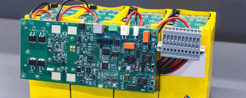
Printed circuit boards (PCBs) are an essential component of modern electronics. They provide a platform for the electronic components to be mounted on and interconnected. PCBs have made electronic devices smaller, more reliable, and less expensive. They have become an indispensable part of our daily lives, from smartphones to cars and airplanes.
A PCB reference design is a blueprint or a template for a specific type of PCB. It provides a starting point for designers to build their own PCBs. The reference design includes the schematic, the layout, and the bill of materials (BOM). It can be used as a guide for selecting components, placing them on the board, and routing the traces. A good reference design can save time, reduce errors, and improve the performance of the final product. It can also ensure compatibility with other systems and standards.
What is a PCB Reference?
A PCB reference is a standardized and well-documented printed circuit board (PCB) design that serves as a benchmark or starting point for other PCB designs. It is a reference design that can be used as a template or guide for designing other PCBs, and it can help to ensure that the resulting PCBs are reliable, efficient, and cost-effective.
A PCB reference typically includes information on the layout, routing, component placement, and other important aspects of the PCB design. It may also include information on the materials, manufacturing processes, and testing procedures used in the design.
Using a PCB reference can save time and effort in the design process, as designers can start with a proven design and make modifications as needed to meet their specific requirements. It can also help to ensure consistency and quality across different PCB designs, particularly in large-scale production environments.
However, it is important to note that a PCB reference is not a one-size-fits-all solution. Different applications may require different PCB designs, and designers should carefully evaluate their specific requirements before using a reference design. Additionally, PCB references should be regularly updated and reviewed to ensure that they remain relevant and effective.
Overall, a PCB reference can be a valuable tool for PCB designers, but it should be used judiciously and in conjunction with careful evaluation and analysis of specific design requirements.
Uses of PCB Reference
PCB reference is a vital tool in the electronics industry. It is a reference point that helps designers, engineers, and manufacturers to build high-quality printed circuit boards. Here are some of the uses of PCB reference:
1. Accurate Component Placement
PCB reference helps in the accurate placement of components on the board. The reference points are used to align the components with the board’s design. This ensures that the components are placed in the right position and orientation, preventing any misalignments that can cause the board to malfunction.
2. Precise Drilling
PCB reference is also used to ensure precise drilling of holes on the board. The reference points are used to guide the drilling machine, ensuring that the holes are drilled in the right location and at the right depth. This prevents any damage to the board and ensures that the components fit perfectly.
3. Consistent Production
PCB reference is crucial for consistent production of printed circuit boards. The reference points ensure that every board is manufactured to the same specifications, reducing the chances of errors and defects. This also helps to improve the quality of the boards and reduces the time and cost of production.
4. Quality Control
PCB reference is also used in quality control to ensure that the boards meet the required standards. The reference points are used to check the accuracy of the component placement, drilling, and other manufacturing processes. This helps to identify any defects or errors and ensures that the boards are of high quality.
In conclusion, PCB reference is an essential tool in the electronics industry. It helps to ensure accurate component placement, precise drilling, consistent production, and quality control. By using PCB reference, designers, engineers, and manufacturers can build high-quality printed circuit boards that meet the required standards.
Types of PCB Reference

There are several types of PCB reference that are commonly used in the industry. These include:
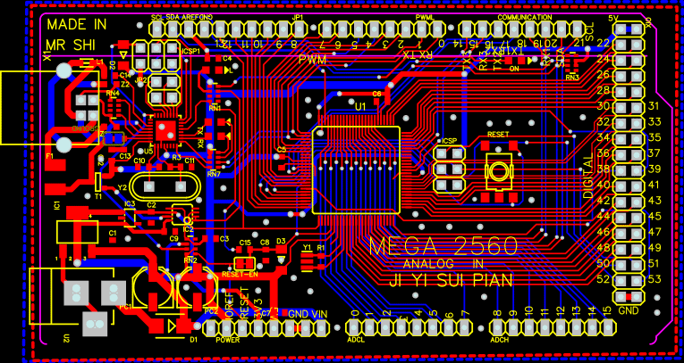
1. Silk Screen
Silk screen is the most common type of PCB reference. It is a printed label that is placed on the PCB to identify the components and their locations. The silk screen is usually printed in white ink on a green background, but it can also be printed in other colors.
2. Assembly Drawing
An assembly drawing is a detailed drawing that shows the location of each component on the PCB. It is usually created by the designer and provided to the manufacturer to ensure that the PCB is assembled correctly.
3. Schematic
A schematic is a diagram that shows the electrical connections between components on the PCB. It is used to design the PCB and to troubleshoot any problems that may arise during testing.
4. Bill of Materials (BOM)
A bill of materials is a list of all the components that are required to build the PCB. It includes the part number, description, quantity, and supplier information for each component.
5. Reference Designator
A reference designator is a code that is used to identify each component on the PCB. It is usually a combination of letters and numbers, such as C1 or R2. The reference designator is used in the schematic, assembly drawing, and bill of materials to ensure that the correct component is installed in the correct location.
In conclusion, understanding the different types of PCB reference is important for designing and manufacturing high-quality PCBs. By using the appropriate reference, designers and manufacturers can ensure that the PCB is assembled correctly and functions properly.
How to Choose the Right PCB Reference
When designing a printed circuit board (PCB), choosing the right reference is crucial. A PCB reference is a specific point on the board that is used as a baseline for all other measurements. It is important to choose the right reference to ensure accurate measurements and proper functionality of the board.
Here are some tips on how to choose the right PCB reference:
-
Choose a stable reference point: The reference point should be stable and not change over time. This ensures that the measurements taken from the reference point remain accurate throughout the life of the PCB. A good reference point is a through-hole via that is connected to a ground plane.
-
Choose a reference point close to the signal: The reference point should be as close as possible to the signal being measured. This reduces the effects of noise and interference on the measurement. A good reference point is a via that is located near the trace carrying the signal.
-
Choose a reference point with low impedance: The reference point should have a low impedance to reduce the effects of noise on the measurement. A good reference point is a via that is connected to a large ground plane.
-
Consider the type of measurement: The type of measurement being taken should also be considered when choosing a reference point. For example, if the measurement is a DC measurement, a stable reference point with low impedance is important. If the measurement is an AC measurement, a reference point with low inductance is important.
-
Follow the manufacturer’s guidelines: Finally, it is important to follow the manufacturer’s guidelines when choosing a reference point. The manufacturer may have specific recommendations for the type of reference point to use based on the design of the PCB.
By following these tips, you can choose the right PCB reference and ensure accurate measurements and proper functionality of your PCB.
PCB Reference Design Guidelines
When designing a printed circuit board (PCB), following proper design guidelines is crucial to ensure its functionality, reliability, and manufacturability. Here are some reference design guidelines to keep in mind when designing your PCB:
Component Placement
The placement of components on the PCB is critical to ensure optimal performance and signal integrity. Here are some guidelines to follow:
- Place components on the same side of the board as much as possible to reduce the number of vias and simplify the design.
- Group components based on their function and signal flow to minimize the length of traces and reduce noise.
- Keep high-speed components, such as microcontrollers and memory, away from noisy components, such as power supplies and motors.
- Place decoupling capacitors as close as possible to the power pins of the components they are decoupling.
Trace Routing
The routing of traces on the PCB is also critical to ensure signal integrity and reduce noise. Here are some guidelines to follow:
- Use wider traces for high-current signals to reduce resistance and avoid overheating.
- Keep traces as short and direct as possible to reduce the risk of interference and signal loss.
- Avoid right angles and use 45-degree angles instead to reduce reflections and signal distortion.
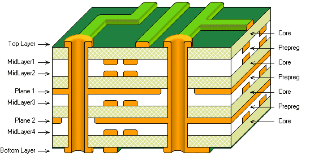
- Use ground planes and power planes to provide a low-impedance return path for signals and reduce noise.
PCB Layout
The layout of the PCB is critical to ensure manufacturability and reduce cost. Here are some guidelines to follow:
- Use standard PCB sizes and shapes to reduce waste and cost.
- Leave enough space between components and traces to allow for easy assembly and inspection.
- Follow the manufacturer’s recommended minimum trace and space widths to ensure manufacturability.
- Use copper pours to reduce the risk of overheating and provide a low-impedance return path for signals.
By following these PCB reference design guidelines, you can ensure that your PCB design is functional, reliable, and manufacturable.
PCB Reference Layout Techniques
When designing a printed circuit board (PCB), it is important to consider the layout techniques that will be used. The layout of a PCB can significantly impact its performance, reliability, and manufacturability. Here are some key PCB reference layout techniques to keep in mind:
1. Component Placement
The placement of components on a PCB is critical for proper functionality. Components should be placed in a way that minimizes noise, reduces interference, and optimizes signal flow. Grouping components by function can also help to simplify the design and reduce the length of traces.
2. Trace Routing
The routing of traces on a PCB is important for signal integrity and reliability. Traces should be kept as short as possible to minimize signal loss and interference. High-speed signals should be routed with controlled impedance to prevent reflections and crosstalk. Signal integrity can also be improved by using differential pairs and avoiding sharp corners.
3. Grounding and Power Planes
Proper grounding and power distribution are critical for noise reduction and signal integrity. Ground planes should be used to provide a low-impedance return path for signals and to reduce EMI. Power planes can be used to distribute power and reduce voltage drop. It is also important to ensure that the ground and power planes are properly connected to the rest of the circuit.
4. Thermal Management
Heat dissipation is an important consideration for high-power applications. Thermal vias can be used to transfer heat from the surface of the PCB to internal layers. Heat sinks can also be used to dissipate heat from components. It is important to ensure that the thermal management system is properly designed to prevent overheating and component failure.
In conclusion, the layout techniques used in PCB design can significantly impact the performance, reliability, and manufacturability of the final product. By carefully considering component placement, trace routing, grounding and power planes, and thermal management, designers can create high-quality PCBs that meet the needs of their applications.
PCB Reference Placement Considerations
When designing a printed circuit board (PCB), reference placement is a crucial consideration. A reference designator is a unique identifier assigned to each component on a PCB. Proper reference placement ensures that components are correctly identified and located during assembly and testing.
One important consideration is the spacing between reference designators. The IPC-7351 standard recommends a minimum spacing of 1.5mm between reference designators to ensure clear identification. If the spacing is too small, it can be difficult to read the reference designators and locate components during assembly.
Another consideration is the orientation of reference designators. It is recommended that reference designators be placed next to the component, rather than on top of it, to avoid obscuring the component markings. Additionally, reference designators should be oriented in the same direction as the component orientation for ease of identification.
When placing reference designators, it is also important to consider the layout of the PCB. Reference designators should be placed in a logical order that corresponds with the layout of the PCB. This can help to reduce confusion during assembly and testing.
Finally, it is important to ensure that reference designators are clearly visible and legible. This can be achieved through the use of bold text, larger font sizes, and contrasting colors. Additionally, the use of a consistent format for reference designators can help to improve readability and reduce errors during assembly and testing.
In summary, proper reference placement is essential for the successful assembly and testing of a PCB. Considerations such as spacing, orientation, layout, and visibility should be taken into account when designing a PCB to ensure that reference designators are clear and easily identifiable.
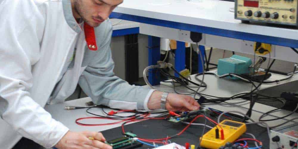
PCB Reference Troubleshooting Tips

When it comes to printed circuit boards (PCBs), it’s not uncommon to run into issues that require troubleshooting. Here are some tips to help you identify and solve common PCB problems:
Check for Short Circuits
One of the most common issues with PCBs is short circuits. These occur when two or more points on the board that shouldn’t be connected are, in fact, connected. To check for short circuits, use a multimeter to test for continuity between different points on the board. If you find a connection where there shouldn’t be one, use a soldering iron to remove the excess solder and separate the two points.
Inspect for Cold Joints
Another common issue with PCBs is cold joints, which occur when the solder joints between components and the board are not properly heated or cooled. To inspect for cold joints, visually inspect the solder joints on the board. If you see any that are dull or have a rough texture, they may be cold joints. Use a soldering iron to reheat the joint and ensure proper adhesion.
Check for Component Placement
Sometimes, PCB issues can be caused by incorrect component placement. Double-check that all components are in the correct place and orientation, and that they are properly secured to the board. If you find any components that are out of place, use a desoldering tool to remove them and reposition them correctly.
Test Power and Signal Lines
Finally, make sure to test the power and signal lines on the board to ensure that they are functioning properly. Use a multimeter to test for voltage and continuity on all lines, and replace any components that are not functioning as they should.
By following these troubleshooting tips, you can identify and solve common PCB issues and ensure that your board is functioning properly.
