The addition of a silkscreen layer to a board is the final step during the manufacturing process of printed circuit boards. The silkscreen layer helps in applying ink traces. This goes a long way in detecting warning symbols, test points, PCB components, marks, logos, etc. Majorly, manufacturers utilize silkscreen during the component part. Basically, silk layer PCB assists designers and manufacturers to quickly identify components.
The ink for silkscreen is an epoxy non-conductive ink. It is also highly formulated. The PCB silkscreen colors are three in number. These are yellow, white, and black. In addition, the software for PCB includes standard fonts in the silkscreen layers. However, you may still choose other fonts.
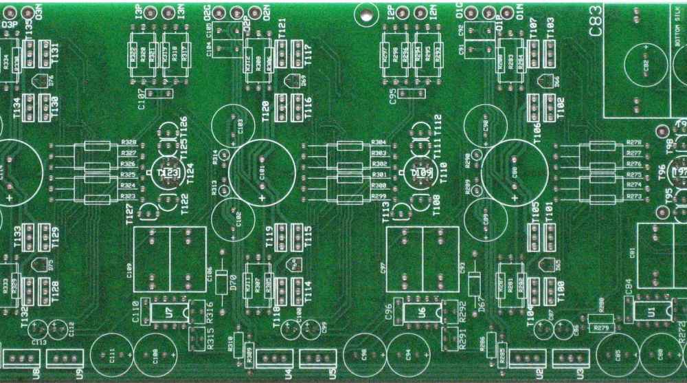
Silkscreen PCB: What is this?
Consider streets and roads of Google maps that have no landmarks and texts to offer more direction. Does this make any sense? Of course, No! Now, PCB silkscreen functions the same way as text and landmarks does. It provides information (text-based) concerning different parts, circuit points, and additional circuitry, with respect to the requirement.
With technology experiencing modern advancement, silkscreen PCB offers beautification images or pictures in an artwork design. Regarding this, you must not overlook the major role of the design and make it difficult to read the information.
Now, you have some understanding about PCB silkscreen. Let’s go ahead to consider its significance or the role it plays.
————————————————————————————
Request PCB Manufacturing Quote , Pls Send PCB Files to Sales@raypcb.com Now
————————————————————————————
Importance of PCB Silkscreen
In order to lay the right background on a silkscreen PCB role, it is important that we recall the uses of a printed circuit board (PCB). PCB offers mechanical support and helps in connecting electronic components. PCBs have signal traces, conductive pathways, or copper sheet-etched traces that are laminated to a substrate (non-conductive).
The conductive tracks and components of the PCB are seen throughout the board without the right identification. This is why it is necessary for end-users and manufacturers to exist. This helps them to identify components such as:
- Manufacturer identifiers
- Testing points
- Warning signs like high voltage
- Processing types
- Version numbers like V2, V3, etc.
- Component orientation and numbers
- Company logos i.e. manufacturer name
The importance and roles of silkscreen PCB include:
- Identifying circuit points such as part interconnect, testing points, etc. quickly
- Useful in troubleshooting circuits in case you get a defective component or a contrasting outcome
- It helps you quickly identify components whenever you are designing or replacing evaluation requirements.
- It serves as a form of safety by showing some warning signs, such as grounding, high voltage, etc.
- Silkscreen PCB also helps manufacturers dung marketing and branding purposes. However, it prevents illegal duplication or forgery of circuit designs.
Silkscreen PCB is also great for evaluating products, such as rating verifications. Note that the information of your silkscreen depends on the size of your board. If your silkscreen board is a small one, make sure you take the important information seriously.
The process of PCB silkscreen will affect the overall quality of your printed circuit board.
Process of PCB Screen Printing
PCB screen printing can be seen as a solder masking sub-process and others such as UV exposure, development, and baking. The whole silkscreen board printing process is composed of 32 steps. However, we can group them further into five. These processes differ with respect to expenses, quality requirements, and PCB material.
————————————————————————————
Request PCB Manufacturing Quote , Pls Send PCB Files to Sales@raypcb.com Now
————————————————————————————
Designing the PCB Silkscreen
Here, you prepare the designed artwork you wish to print on the board. You then use EAGLE (a computer software) to conduct the process. The section of the silkscreen lets you design your circuitry, silkscreen layer, as well as other elements of design. Once you pick a menu for your silkscreen you can go on with the design
Preparing the board
Once you have completed the CAD blueprint, then you can implement the hardware. Here, you should follow some steps.
- Choose the type of board for the production
- Clean and tape roll it, and handle properly to prepare the board for printing
- Print your prepared design on a transparent paper
- Place them the exact way you want it to look on your PCB
- Maintain the paper of the PCB design in its initial position
- Let the entire setup face downwards
- Use opaque cardboard to cover the setup’s upper part
- Let the lower part be exposed to UV light for about 15 minutes. This helps to develop the silkscreen artwork completely
Silkscreen Printing
This is the actual printing. Follow these steps
- Place your etched PCB underneath your silkscreen fabric
- Make sure it aligns properly placing your silkscreen artwork on the top
- Fix your PCB properly making sure it doesn’t move while the application is on
- Apply your silkscreen curable ink utilizing a squeegee on the top of your artwork
- Dry your PCB after about ten minutes using a drying oven.
Handling and inspection procedure
After the silkscreen printing, let it pass through the handling and inspection procedure. This is to ensure the quality of the board is maintained all through the process. The latter ensures that your printed information can be read with human eyes.
Silkscreen Treatment
Here is the final step. You will treat the silkscreen print properly to ensure that it is set for use. You can determine this by the quality of your silkscreen process.
Silk screen printing PCB Methods
Whatever silk screen printing PCB method you use, you must consider factors like silkscreen board spacing, silkscreen board material, precision, cost, time, etc. We won’t be discussing these factors for now. However, we will be considering the silk screen printing PCB methods.
Manual Screen Printing
The manual screen printing is the oldest silk screen printing PCB method. To conduct this process, you must utilize epoxy ink. Generally, what you do is to insert the link to get to the laminate. Next, you dry iy to get that impression on the silk layer PCB.
One great advantage of the manual silkscreen board printing is that you can manage its setup requirements more compared to others. This is why most tasks prefer this option. Also, this method requires a large silkscreen board size, as well as impression drying. This is so due to the larger size of text that is dominant with this method.
To reduce expenses, it is advisable to make use of the manual screen method of printing. Also, with this method, board spacing won’t become an issue.
————————————————————————————
Request PCB Manufacturing Quote , Pls Send PCB Files to Sales@raypcb.com Now
————————————————————————————
Direct Legend Printing
This method of printing makes use of a similar principle as the paper printer. This would be of great assistance if you possess inkjet printers (high-end) that can transfer ink to boards. One great benefit of using this method is that the application information of your CAD is printed directly to the board. In addition, innovators have upgraded the ink used for this printing to acrylic. This upgrade was necessary when you consider the drying time.
This screen printing method is also a modern one. It comes with time efficiency and high accuracy features. Also, the plan has low heights, which are usually equal to or above 0.02 inches. Avoid applying any height that is below 0.02 because the human eye may be unable to read it.
The disadvantage of this silk screen printing PCB method is that you can’t utilize it for printed circuit boards having silver materials. Furthermore, acrylic ink poses some restrictions in some cases.
Generally, choosing the right silk screen printing PCB method goes a long way in saving time and cost.
Liquid Photo Imaging
For this type of silk screen printing PCB, the laminate is first coated via the epoxy. The epoxy is referred to as a liquid having properties of photo imaging. Next, you transfer your silkscreen sketch through UV light exposure to plates.
The results of liquid photo imaging have a better precision compared to those done manually. Besides, you need less space for this method in contrast to the manual type. However, this method uses up more setup time and ink compared to other methods of screen printing.
We advise that you choose this silk screen printing PCB method whenever you wish to save PCB fineness and space.
Silkscreen PCB Design Guidelines
Concerning silkscreen, there are different designs. This varies from the simple ones to the complex designs. If you fail to include the necessary and adequate information during the silkscreen PCB design, then it can be seen as having little landmarks and knowledge when using Google Maps. In this scenario, the travelers will get lost easily. To avoid this, work with these guidelines to help you in using your silkscreen maximally.
Ask your PCB manufacturer questions concerning the method used when manufacturing silkscreen
Majority of manufacturers cannot produce silkscreen utilizing all the methods of three-screen printing. Therefore, reach out to any manufacturer of your choice, and make enquiries about the manufacturing capacity of their silkscreen. The method used affects the primary elements of your design like size clearance, traces, component pads, vias, and silkscreen marking location.
During the PCB layout, make sure you account for the silkscreen items
To make your silkscreen readable, markings like pin one, reference indicators, and polarity should stay adjacent to any related component. As you make the design, also take note of the extra spacing requirements. This is to prevent the indicators from covering or overlapping.
Select your fonts to work in line with the printing method your manufacturer uses
There are PCB design packages that allow users to make virtually all font styles of silkscreen. However, there are manufacturers that can only use a few of those fonts. This is why you must ask your service provider and be sure you are including fonts that your manufacturer supports.
Don’t overuse silkscreen markings
At times, there may be temptations to make use of signs for all components, as well as other imagery which could prove useful during testing, assembly, repair, using the final product. However, with the present demand for compact and miniaturized boards, including almost all the available information is almost not possible.
Regarding this, make sure you prioritize your markings using these descriptions.
- Begin with some regulatory requirements such as lead-free labeling required by J-STD-609A Labeling and Marking of Components, PCBAs, and PCBs to help in identifying Lead-Free, Lead, as well as other aspects of IPC.
- Second, consider the markings and identification of the manufacturer such as component number of the PCB, labels, company logo, and serial number.
- Third, prioritize the assembly aids like pin one indicators and polarity. Also, include reference indicators that work in line with the board space available.
- Lastly, consider some tasting aids such as jumper and point indicators
If you can prioritize the marking using the guide given above, then you will for sure make great use of the labeling and identification of your PCB. This also holds even when you use a small board.
————————————————————————————
Request PCB Manufacturing Quote , Pls Send PCB Files to Sales@raypcb.com Now
————————————————————————————
DIY PCB Silkscreen
Here, there are some points to look into to ensure a successful and perfect DIY PCB silkscreen. The first thing to note here is applying the PCB CAD tool. This is necessary for designing the text placement, font, and color.
This is called artwork. Artwork is a very important part during the silkscreen. There’s a need to utilize a creative and directional approach to ensure your board looks appealing as well as readable.
Also, learn about the transfer of the ink laminate. This process is elusive and surely impacts your final product directly. For the ink laminate to be transferred, stretch the polyester screens and then coat them. If you don’t position your panels and screens simultaneously, you may eventually bring damage to the whole PCB. Immediately you complete the process of coating, make sure you dry it properly before using it.
However, while doing DIY PCB silkscreen, there are aspects that may require you to seek help from a manufacturer. Therefore, if you want a professional job done, reach out to a reliable manufacturer.
Conclusion
The process of PCB silkscreen is delicate. This is because the quality of the printed circuit board can be affected. Another aspect you must consider closely is the cost aspect during the design. Furthermore, having a good understanding about the whole process of screen printing as well as the benefits and pitfalls of each of the printing methods ensures that it becomes easy to decide if you should do a DIY PCB silkscreen or consult the services of any professional manufacturer.
Contact us today if you wish to need the manufacturing of your silkscreen design to be done professionally.
