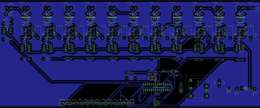
A 4 channel relay PCB layout is a critical component in any electronic circuit design. It helps to control multiple devices and systems at the same time, making it an essential tool for engineers and designers. The layout of the PCB is crucial in ensuring that the system operates efficiently and effectively.
When designing a 4 channel relay PCB layout, it is essential to consider the various factors that can affect its performance. These factors include the size of the board, the spacing between the components, and the placement of the traces. A well-designed PCB layout can help to minimize signal interference, reduce noise, and improve overall system performance.
Basics
What is a 4 Channel Relay PCB?
A 4 channel relay PCB is a printed circuit board that contains four relays. A relay is an electronic switch that can be used to control a circuit. Each relay on a 4 channel relay PCB can be controlled independently, allowing the user to switch four different circuits on and off.
Why is PCB Layout Important?
The layout of a PCB is important because it can affect the performance of the circuit. A good PCB layout can minimize noise and interference, while a bad layout can cause problems such as signal degradation and electromagnetic interference.
When designing a PCB layout for a 4 channel relay PCB, it is important to consider the following:
-
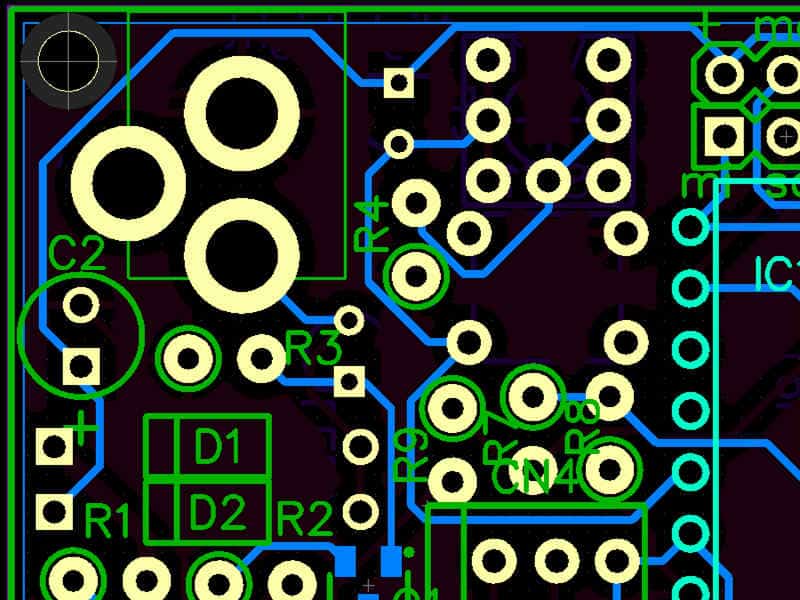
Component placement: The placement of components on the PCB can affect the performance of the circuit. For example, placing components too close together can cause interference between them.
-
Signal routing: The routing of signals on the PCB can affect the quality of the signal. It is important to keep signal traces as short as possible and to avoid routing them near noisy components.
-
Grounding: Proper grounding is essential for minimizing noise and interference. It is important to ensure that all components are properly grounded and that the ground plane is continuous.
Overall, a well-designed PCB layout can improve the performance and reliability of a 4 channel relay PCB.
Design Considerations

When designing a 4 channel relay PCB layout, there are several important considerations to keep in mind. These include power supply, signal traces, component placement, and ground planes.
Power Supply
The power supply is a critical aspect of any PCB design, and the 4 channel relay PCB is no exception. It is important to ensure that the power supply is stable and reliable, and that it can provide sufficient current to the relays. A regulated power supply is recommended to ensure that the voltage does not fluctuate.
Signal Traces
Signal traces carry the signals between the components on the PCB. It is important to ensure that the signal traces are kept as short as possible to minimize interference and signal loss. The width of the traces should also be carefully considered to ensure that they can handle the required current without overheating.
Component Placement
The placement of components on the PCB can have a significant impact on its performance. It is important to carefully consider the placement of the relays, as well as any other components that may be affected by the switching of the relays. Components should be placed to minimize noise and interference, and to ensure that the PCB is as compact as possible.
Ground Planes
Ground planes are an important aspect of any PCB design, and they are particularly important in the case of a 4 channel relay PCB. A solid ground plane can help to reduce noise and interference, and it can also help to dissipate heat. It is important to ensure that the ground plane is connected to all of the components on the PCB, and that it is as large as possible to minimize resistance.
In summary, when designing a 4 channel relay PCB layout, it is important to carefully consider the power supply, signal traces, component placement, and ground planes. By paying close attention to these factors, it is possible to create a reliable and high-performance PCB that meets the needs of the application.
Tips and Tricks
Keep Traces Short
When designing a 4 channel relay PCB layout, it is important to keep your traces as short as possible. Long traces can increase resistance and capacitance, leading to signal degradation and potential interference. By keeping traces short, you can minimize signal loss and improve the overall performance of your design.
Use Appropriate Trace Widths
Another important factor to consider when designing a 4 channel relay PCB layout is trace width. The width of your traces will determine how much current they can carry. It is important to choose an appropriate trace width to ensure that your design can handle the necessary current without overheating or causing damage.
Avoid Crosstalk
Crosstalk is a common problem in PCB design that occurs when signals from one trace interfere with signals on another trace. To avoid crosstalk in your 4 channel relay PCB layout, it is important to keep your traces spaced apart and to use ground planes and shielding when necessary.
Test the Design
Before finalizing your 4 channel relay PCB layout, it is important to test the design to ensure that it meets your specifications. This can include testing for signal integrity, power consumption, and overall performance. By testing your design, you can identify and address any potential issues before they become a problem.
Following these tips and tricks can help you design a high-performance 4 channel relay PCB layout that meets your needs and specifications.
Conclusion
In conclusion, designing a 4 channel relay PCB layout requires careful consideration of various factors such as the size of the board, the number of components, and the voltage and current requirements. A well-designed PCB layout ensures that the relay operates efficiently and reliably.
Throughout the design process, it is important to keep in mind the safety of the end-users by incorporating safety features such as overcurrent protection and isolation barriers. Additionally, it is essential to follow industry standards and guidelines to ensure the reliability and longevity of the PCB.
When designing a 4 channel relay PCB layout, it is important to consider the purpose of the relay and the specific application it will be used for. This will help determine the appropriate components and design specifications needed to meet the desired functionality.
Overall, designing a 4 channel relay PCB layout requires a thorough understanding of the components and their interactions with each other. With careful planning and attention to detail, a reliable and efficient PCB can be designed to meet the needs of any application.
