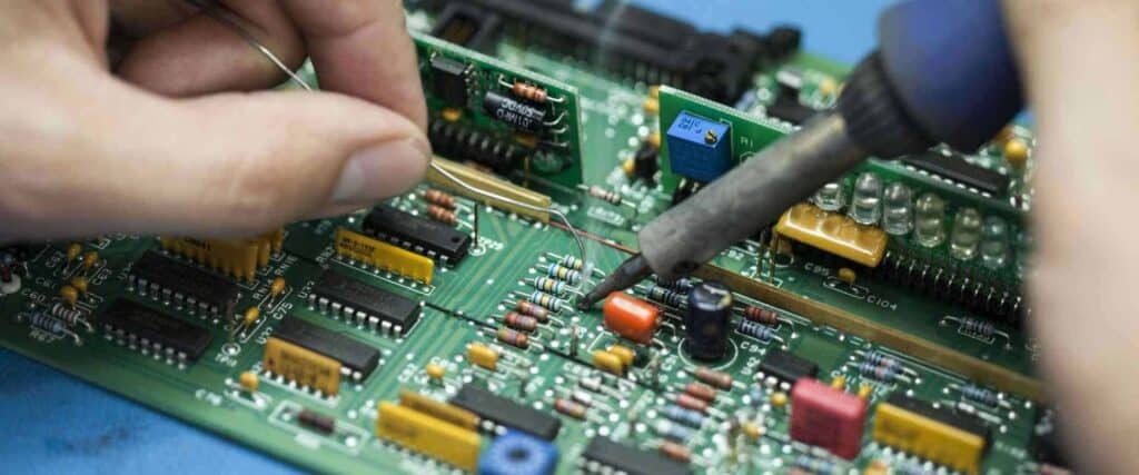
Printed Circuit Assembly (PCA) is an essential process in the electronics industry, where components are mounted on Printed Circuit Boards (PCBs) to create functional devices. The quality of these assemblies is critical to the performance and reliability of the devices they are utilized in. To ensure optimal results, there are several aspects to consider during the assembly process that can have significant impacts on the final product.
First and foremost, the design of the PCB, the selection of components, and the choice of a suitable assembly method play vital roles in creating a quality PCA. By focusing on these aspects, manufacturers can minimize potential issues and improve overall efficiency. Additionally, proper inspection techniques and testing procedures are vital in enhancing the performance and life of the assembled product.
Moreover, it is crucial to maintain cleanliness and controlled environmental conditions during the assembly process to prevent contamination and ensure an effective soldering process. Considering these points can ultimately lead to a more reliable and efficient PCA, which is essential for the smooth functioning of the end product in various applications.
Design for Manufacturability
Component Selection
When selecting components for a printed circuit assembly (PCA), it is essential to consider factors such as availability, compatibility, and cost. Choosing readily available components with a reliable supply chain can reduce lead times and minimize production delays. Also, ensure that the chosen components are compatible with the design requirements and meet performance expectations.
PCB Layout
A well-designed PCB layout is crucial for manufacturability, as it directly affects the ease of assembly and overall functionality. Some key considerations for PCB layout are:
- Maintain adequate spacing between components to prevent soldering issues and facilitate inspection and debugging.
- Minimize the usage of vias, as they can lead to additional manufacturing steps and increase costs.
- Utilize a uniform and logical component placement strategy, minimizing track lengths and reducing the likelihood of errors during assembly.
Thermal Management
Proper thermal management is vital in PCB design to ensure that components operate within their specified temperature range, preventing premature failures or reduced performance. Some techniques for improving thermal management include:
- Incorporating heat sinks and thermal vias to dissipate heat away from critical components.
- Utilizing appropriate PCB materials, such as those with a high thermal conductivity, to facilitate heat transfer.
- Designing with thermal considerations in mind, such as placing temperature-sensitive components further away from heat-generating components.
By adhering to these guidelines when designing for manufacturability, you can create robust and efficient PCA designs that are cost-effective and straightforward to assemble.
Solder Paste Application
Stencil Design
Stencil design plays a critical role in the solder paste application process. The stencil acts as a template for ensuring proper solder paste application on the Printed Circuit Assembly (PCA). Here are some factors to consider when designing stencils:
- Aperture size and shape: Design the apertures according to the component footprint to achieve good solder joint quality.
- Stencil thickness: Balance the stencil thickness to achieve the desired solder paste volume without causing bridging or insufficient solder.
- Material selection: Choose materials like stainless steel or nickel to provide durability and stability during the solder paste application process.
Solder Paste Type
Selecting the right solder paste type is essential for ensuring a high-quality PCA. There are different types of solder paste available, and the choice depends on your specific requirements:
- Leaded solder paste: Contains lead and is typically used when lead-free soldering is not mandatory. Leaded solder paste provides good solder joint strength and is easy to work with.
- Lead-free solder paste: Lead-free solder paste contains other alloys, like tin-silver-copper (SAC), and must be used when required by regulations or customer specifications. This type of solder paste has a higher melting point and may cause more stress on the PCA during the soldering process.
When choosing a solder paste type, it’s essential to consider factors like alloy composition, reflow profile compatibility, and performance requirements to ensure optimal solder joint quality in the final assembly.
Pick and Place Process

Component Alignment
The component alignment process is crucial to ensure the proper operation of the Printed Circuit Assembly (PCA). During this process, the machine aligns the components on the printed circuit board (PCB) before placement. A few points to consider during component alignment are:
- Utilizing high-quality vision systems to enhance alignment accuracy
- Regularly monitoring and calibrating the vision equipment
- Ensuring compatibility between the component feeders and the pick and place machine
Placement Accuracy
Placement accuracy is another essential aspect of the pick and place process, as it directly affects the functionality of the PCA. Several factors contribute to achieving high placement accuracy, such as:
- Implementing precise motion control systems, such as linear motors, for accurate component placement
- Consistently monitoring machine performance and conducting regular maintenance
- Adhering to the manufacturer’s recommendations for machine parameters, such as speed and pressure
In summary, focusing on component alignment and placement accuracy in the pick and place process leads to more reliable and efficient Printed Circuit Assembly. Employing high-quality equipment, adhering to manufacturer recommendations, and regular monitoring are vital to achieving this goal.
Reflow Soldering
Temperature Profile
Reflow soldering is a crucial process in printed circuit assembly, and maintaining an appropriate temperature profile is important for reliable solder joints. There are four main stages in the reflow soldering process:
- Preheat: Gradually raising the temperature of the PCB to avoid thermal shock.
- Soaking: Allowing the temperature to stabilize, ensuring that all components reach a uniform temperature.
- Reflow: The solder paste reaches its peak temperature and forms solid connections between the components and the PCB.
- Cooling: Rapidly cooling the PCB to solidify the solder and ensure proper joint formation.
It’s important to follow the manufacturer’s recommended temperature profile, as deviating from this can cause defects and reduce the reliability of the solder joints.
Managing Warping
Warping, or bowing, is a common issue that can occur during the reflow soldering process. To minimize warping during assembly, consider the following factors:
- Material selection: Choose PCB materials with low thermal expansion coefficients that are less prone to warping.
- Board thickness: Thicker boards are generally more resistant to warping, so consider increasing the thickness if warping is a concern.
- Preheat rate: A slower preheat rate can help reduce warping by ensuring even heat distribution throughout the PCB.
- Solder mask type: Using a flexible solder mask material can help mitigate warping by allowing the PCB to expand and contract more easily during the reflow process.
- Component placement: Uniform component distribution across the PCB can help avoid localized stress and reduce the risk of warping.
By carefully considering these factors and following proper reflow soldering guidelines, you can ensure quality and reliable printed circuit assembly results.
Inspection and Testing
Automated Optical Inspection
Automated Optical Inspection (AOI) is a crucial step in the Printed Circuit Assembly (PCA) process. It uses high-resolution cameras and advanced software algorithms to detect defects on the assembled PCB. AOI checks for:
- Component presence, absence, or misalignment.
- Solder paste volume and quality.
- Solder joint quality.
The AOI process helps reduce the risk of failures and ensures overall assembly quality.
X-ray Inspection
X-ray Inspection is another important technique for inspecting PCA. This method uses X-ray technology to examine the inside of PCB assemblies, which is especially useful for BGAs (Ball Grid Arrays) and hidden joints. The main benefits of X-ray Inspection include:
- Detection of solder bridges and voids.
- Inspection of solder joint integrity and wire bonds.
- Examination of PCB layers for proper alignment, shorts, and opens.
By employing both AOI and X-ray Inspection techniques, a comprehensive examination of every PCA is achieved, ensuring high-quality and reliable end products.
Common PCB Assembly Errors
Solder Bridges
Solder bridges occur when solder connects two or more adjacent pins, causing unintentional electrical connections. This can result in short circuits and may damage the PCB. To avoid solder bridges, ensure the proper soldering temperature, flux type, and solder mask.
- Maintain appropriate soldering temperature
- Choose the right flux type
- Apply solder mask effectively
Tombstoning
Tombstoning is a phenomenon where a surface mount component stands up vertically on one end, resembling a tombstone. This occurs due to uneven heating during reflow soldering or component placement misalignment. Tombstoning can cause open circuits and reduce the reliability of the PCB.
| Cause | Prevention Measures |
|---|---|
| Uneven heating | Monitor reflow profile |
| Misalignment | Fine-tune component placement |
| Component size | Select compatible components |
Voiding
Voiding refers to the presence of gaps or air pockets within solder joints, decreasing their structural integrity and electrical conductivity. Voiding occurs due to several factors such as poor solder paste application or inadequate solder temperature.
- Proper solder paste application
- Optimal solder temperature
- Adequate outgassing during the solder reflow process
