A Complete Guide on PCB Layers
Can you visualize starting a new road construction from rigid paving and transition? That sounds absurd right? Constructing a road project usually begins with concept planning and funding. The effect of such a project on the environment is then considered. This involves all likely damages the project could cause the environment. All other steps will follow in sequence until the project gets completed.
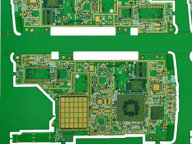
Designing a PCB takes a familiar pattern. It is important to have a solid and logical design concept with the layers at its foundation. A PCB is the sum total of conductive layers in a proper segmented manner. These layers get their names coined out from their functions and positions. A PCB layer includes signal transferring levels which are vertical to the surface of the PCB.
Furthermore, the layers explain the comprehensive operation of the PCB. Thus, it will be disastrous having a PCB designed without the PCB layers.
What are PCB Layers?
A PCB is a coated display board that consists of transmitting and insulating surfaces. It also means the total number of conductive layers in an arranged order. The conductive layers are the Signal bases from which current goes through to other parts of the PCB.
The PCB has its classifications based on the copper layer counts. It might be a one or two board layer. 1 layer PCB is also known as single sided PCB as well as two layers called double sided PCB. The double sided PCB has the lid and base layers while PCBs with 4 layers have two extra inner surfaces added.
Furthermore, the addition of extra PCB layers enhances the proficiency of the board. It annihilates electrostatic obtrusion, helps power distribution and propels signals at high speed. The choice in numbers of PCB layers used is dependent on the purpose of its design.
PCB Layers Components
The following are the components of the PCB layers
Dielectric Materials
Dielectric materials direct nominal electricity and supply coverage between two surfaces. They aid in separation of signals within PCB layers. Also, they track regular interruption over a wide wavelength.
Copper
The role played by copper in the PCB is undeniable. Outside of being a great carrier of electricity, it performs other functions as well. The copper on the PCB layers influence the ability of the PCB to receive suitable current flow. It also controls loss of power on the circuit board.
In a bid to regulate interruptions and voltage on the plane board, the standard of the copper is crucial. This standard influences the durability of the PCB. However, the PCB can become more stable through merger of copper’s density and length.
Trace Dimensions
This is an important component on the PCB layer. The role played by the dimensional trace is to define the area of the board and its mechanical layer. It also gives the basic evaluation of the board which helps in placing the elements on the PCB layer.
PCB Layers Explained
The PCB is a platform by which electric elements get connected to electrical devices. Pointing out that the PCB is basically designed of copper, coating and resin is important. A quality circuit board has an overlay surface of copper coated between layers of transmitting elements.
In making a choice of PCB design, the type of PCB layer required to fabricate a standard PCB must be the foremost. Also, understanding that cost is not the sole factor to consider in choosing a PCB layer is vital.
The wave frequency is also an important factor that affects the choice of PCB design in an appliance. Various types of PCB layer exist, though classified into six categories.
PCB Layer Categories
Single-Layer PCB
The single sided circuit board is a perfect design for small electrical appliances. It has a single surface conductive line with coated coverage on one part, while the other part has the electrical components fixed. This type of PCB does not accommodate wire interchange required by high speed gadgets.
Double Layer PCBs
This type of PCB has two transmitting surfaces fixed on both sides of the board. It implies the possibility of wire connection from one surface to another. It is suitable and mostly found in modern electrical gadgets used for multiplex tasks.
Four Layer PCBs
The four layer circuit board allows for diverse product efficiency. It serves as one of the secured alternatives used for PCBs design. This circuit board has four layers of coppers laid together which involves one bottom, top and two inner layers. Connections between these layers are through buried holes, blind holes and through holes.
Six Layer PCBs
The 6 layer PCB is an essential part of the solid dimension types of circuit boards. It consists of 6 layers of transmitting materials. It is an upgrade on the 4 layer rigid flex PCB with two added layers for signals laid in the middle of the flat surface.
A model six layer PCB presents six surfaces. They include two internal, two external layers and two internal planes (for power and ground). This design also enhances electromagnetic interference. It also provides a greater route for modest and excessive pace signals.
8 Layer PCBs
This type of PCB layer is best fit for compact appliances and devices with confined space on the board.
10 Layer PCBs
The 10 layer PCB consists of sufficient spacing for power surfaces and domains. It is the maximal tally of layers that can conveniently fit into a 1mm thickness SODIMM plug.
In view of the variety of options available, making a choice of PCB layer design could be challenging. Even so, irrespective of the type of PCB chosen, each board has a base on which it’s built. Various laminated elements that are vital in any type of PCB layer are further explained as you read on.
Elements of PCB Layer
Substrate Layer
The substrate layer is the foundation on which fabricating a quality PCB stands. The PCB needs a design and frame on which other elements hold on to. It is the visible materials that firm together elements and traces. The quality of the substrate determines the performance of the PCB, thus the need to make a right choice.
The emerging PCB industry has seen the usage of many substrate materials for PCB design. It ranges from solid fiberglass, epoxy aramid, polyimide glass and the flexible polymer. Fiberglass has been the most frequent choice for PCB design due to its reliability and its cost effectiveness.
Nonetheless, substrate materials such as flexible polymers are best suited for flexible PCBs. They do not have the resilience found in fiberglass to produce a super quality board.
Copper Layer
After the substrate material is perfectly fixed on the PCB, the coated copper foil fixing is next. The laminated copper foil goes through a heating process in attaching it to the board. The capacity of the PCB will determine the copper density required. PCBs designed for small gadgets will not need a thickened copper layer.
Soldermask layer
The soldermask performs the function of the insulator. It’s placed over the copper layer to keep the PCB from elements that could disrupt the copper traces.
In order to protect the copper layer from exposure to added metals or components, the need for this layer. It is a crucial layer in the fabricating process, it aids soldering to the right places on the board.
Silkscreen layer
This layer is practically for end users to enable detailed understanding of the PCB. It helps to increase the knowledge of the elements on the board.
The discussed layers exist in all types of the PCB designs. They are significant to the effectiveness of every kind of board.
Layer Board
In relation to Layer Boards, their names include single layer, 2 layers or double layer and the multi-layer PCBs. The tally of layers in digits it possesses forms the number of transmitting layers it has.
The PCB has other layers like the substrate, soldermask, copper, and silkscreen. The total number of layers describes the amount of conductive layers in the PCB. Consequently, a layer board with one transmitting layer is a single layer PCB
A Single Layer Board is the easiest of boards available because it has a single conductive layer. It is popular among the applications where the need for compact layer boards arises. PCB as there is only one conductive layer.
Amidst every kind of layer board, the single layer board tops the preference chat. Producers adopt the multi-layer or double layer boards only when the board is composite. Differently, the single layer board holds the first choice for any gadget or project. The single layer board has various types with unique features.
Types of single layer boards
- Single layer rigid Board
- The single layer flexible Board
- Single layer rigid flex Board
- The single layer high frequency board
- Single layer aluminum board
Double Layer Board
This is the type of Layer board designed with the coated copper layer on each side of the board. Simply put, it means the layer board that has both sides with tracing paths.
The tracing paths on both edges of the double layer board separate it from the single layer board type. Its functionality cuts across ranging electronic gadgets, from simple to complex appliances.
Elements on this layer board secure connections using through-hole or surface mounting. Each technique has its restrictions and benefits.
Furthermore, the double layer board allows for adjacent wire routing. Fastening both layers could be a difficult task, but it could be easily done with the pick and place device. It is speedy approach as compared to the manual process.
Multi-Layer Board
The multi-layer board came up due to the advancements in the electronics industry. The use of electronic gadgets moved from the ordinary to an advanced level over a period of time. This gave birth to a composite board such as the multi-layer board.
The Multilayer board comprises three or more transmitting coated copper layers. They emerge as separate layers of two sided boards, coated and fastened through heat to the layer. The electrical components on the layers secure connections through via.
Furthermore, the cost of producing a multi-layer board is high due to its compounded production process. It is the most complex of all the board layers available, thus it is suitable for high frequency gadgets.
PCB Board Layers
The PCB Board comprises various layers. Detail on each layer is further discussed
Mechanical Layers
The mechanical layer on the board explains the visible size of the board. Fabrication of the board is on the mechanical layer. Though, there are various mechanical layers that form the board. The mechanical layer could appear in a rectangular or tailored structure.
Kept Out Layers
This layer on the board works to compliment the mechanical layer. It sets the maximum designated part on which the board design could stand. The kept out layer is a check factor on the boundaries allocated to the board design.
Ground Planes & Power Planes
They are solid conductive layers conned into a lasting potential. The power plane has its linkage to the DC on the board while the common drain (GND) has its linkage to the ground plane.
Both planes are favorable current and ground conductors among the elements on board. They are present at the upper, inner and lower parts of the PCB. They can enhance the functionality of the PCBs in some circumstances.
Routing Layers
The routing layers perform the interconnecting function between various parts on the board. These layers are present at the upper surface, inside the board as well as the lower surface. It is an important layer in the manufacturing process.
Overlay/Silkscreen Layers
This layer gives the board parts text indicators both on the lower and upper layers. The text indicator is very vital mostly when the PCB needs correction in the laboratory. The Silkscreen layers help in specifying board serial number, name of design and other names on the board.
Solder Mask Layers
The solder mask layer safeguards the copper traces from compressing due to dust. It is mostly designed in green and it covers either the upper or lower side of the PCB.
Solder mask is not on every PCB. Therefore, there has to be indications on the PCB layers that require it. Furthermore, solder masks are virtually tagged negatives. It implies the sides of the PCB that do not need the solder mask.
Conclusion
This article has explained the importance of having layer boards in designing all kinds of PCBs. Layers are the foundation on which other components of the design stand. Elements such as the substrate material, copper, solder mask and silkscreen layers are vital to designing a quality PCBs.
