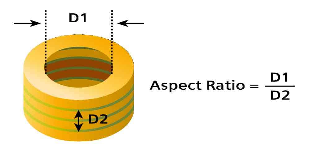
If you’re looking for a perfect guideline about aspect ratio of PCBs, then you have come to the right place. The aspect ratio of a printed circuit board (PCB) is the ratio of the board’s length to its width. In other words, it is the relationship between the length and the width of the PCB.
Aspect ratio is an important consideration in PCB design because it affects the board’s manufacturability and functionality. If the aspect ratio is too high, it can make it difficult to drill holes or create vias in the board. This can impact the board’s overall performance. In contrast, if the aspect ratio is too low, it can limit the density of components on the board.
In general, a “safe” aspect ratio for most PCB designs should be between 1:1 and 5:1. However, this can vary depending on the specific requirements of the design and the capabilities of the manufacturer. It is always important to consult with the manufacturer early in the design process. It is to ensure that the aspect ratio is within their capabilities and to adjust the design for manufacturability.
Factors Affecting the Aspect Ratio of PCB
Printed circuit boards (PCBs) are integral components of many electronic devices. PCBs are providing a platform for electronic components to mount on. The aspect ratio of a PCB is an important consideration when designing and manufacturing a PCB. It can impact the reliability and performance of the board. In this section, we will explore the factors that affect aspect ratio and how they impact the design.
1. PCB Thickness and Layer Count
The thickness and layer count of a PCB are the most fundamental factors that affect the aspect ratio. You can calculate the aspect ratio easily. It is the ratio of the PCB’s thickness to the diameter of the smallest hole. Thus, as the thickness of the PCB increases, the aspect ratio decreases, and vice versa.
The layer count of a PCB can also impact the aspect ratio. Multi-layer PCBs, which have more than two layers of conductive material, typically have smaller aspect ratios. This is because the insulating layers between conductive layers limit the maximum drill depth of the holes or vias.
2. Size and Density of Components
The size and density of components mounted on a PCB can also impact the aspect ratio. Smaller components, such as surface mount technology (SMT) components, are more densely on a PCB. So, it can result in smaller aspect ratios. Larger through-hole components, on the other hand, require larger holes and vias, which can limit the aspect ratio.
The density of components on a PCB can also impact the aspect ratio. High-density PCBs, which have many components in a small area, can require smaller holes and vias for high density. This can result in smaller aspect ratios. This is because the thickness of the PCB limits the depth of the hole or via.
3. Manufacturing Process Capabilities
The manufacturing process used to create a PCB can also impact the aspect ratio. Different manufacturing processes have different capabilities when it comes to creating PCBs with different aspect ratios. For example, the drilling and plating processes to create the holes on a PCB can impact the aspect ratio.
The drilling process for creating holes or vias on a PCB. Engineers do it by using mechanical or laser drilling. Engineers use mechanical drilling for larger holes and vias, while laser drilling for smaller holes and vias. Laser drilling can produce holes and vias with a smaller diameter, which can result in a smaller aspect ratio.
The plating process for creating the conductive layer inside the holes or vias can also impact the aspect ratio. Electroless plating is typically used for smaller holes and vias, while electroplating is used for larger holes and vias. Electroless plating can produce a more uniform and consistent plating layer inside the hole or via. And it can result in a higher aspect ratio.
4. Impact of Aspect Ratio on PCB Design and Manufacturing

The aspect ratio can impact both the design and manufacture of a PCB. A high aspect ratio can result in a more reliable and robust PCB design. It allows for greater depth of the hole or via, which can provide better mechanical stability and thermal performance. However, a high aspect ratio can also make the manufacturing process more challenging. It requires more precise drilling and plating processes.
High aspect ratio PCBs can be more expensive and time-consuming to manufacture. Here, the drilling and plating processes require more time and resources to ensure the holes are of high quality. Additionally, the increased complexity of the manufacturing process can result in a higher rate of defects and lower yields. It can further increase the manufacturing cost and lead time.
5. Communication with the Manufacturer
It is important to communicate with the manufacturer during the design process to manufacture PCB efficiently. This can help to identify potential manufacturing issues early on. Furthermore, it can allow for design changes to improve manufacturability.
When working with a manufacturer, it is important to understand their manufacturing capabilities and limitations. Different manufacturers may have different capabilities when it comes to creating PCBs with different aspect ratios. Therefore, it is important to select a manufacturer that can meet the requirements of the PCB design.
During the design process, consider the tolerances and specifications required for the holes or vias on the PCB. This can help to ensure that the PCB has the desired aspect ratio.
In addition to communication with the manufacturer, it is also important to use design rules and guidelines. Design rules can help to ensure that the PCB design meets the minimum requirements for drilling and plating. Furthermore, it can also help to avoid common manufacturing issues such as breakout and burrs.
Examples of Aspect Ratio in PCB Design
Aspect ratio is an important consideration in the design of printed circuit boards (PCBs). This is because it can have a significant impact on the manufacturability, reliability, and performance of the board. In this section, we will explore some examples of aspect ratio in PCB design.
· Through-Hole Technology (THT)
Through-hole technology (THT) is a traditional method of mounting electronic components onto a PCB. THT components have wire leads that pass through holes in the PCB. The aspect ratio of THT vias can have a significant impact on the reliability and manufacturability of the PCB. If the aspect ratio of the via is too high, it can result in insufficient plating. Later, it can cause the via to break or delaminate. On the other hand, if the aspect ratio is too low, it can result in insufficient solder joint fillet. And it can lead to poor electrical connection and mechanical stability.
· Surface Mount Technology (SMT)
Surface mount technology (SMT) is a more modern method of mounting electronic components onto a PCB. Engineers solder SMT components to the surface of the PCB, which eliminates the need for holes in the board. However, SMT components can also have vias that connect different layers of the board. The aspect ratio of SMT vias can impact the reliability and manufacturability of the PCB. A high aspect ratio can result in insufficient plating, which can cause the via to break or delaminate. A low aspect ratio can result in insufficient solder joint fillet, which can lead to poor mechanical stability.
· High-Speed Design
High-speed design is an important consideration in the design of PCBs for applications such as telecommunications and data storage. High-speed design requires careful attention to the routing of signals to ensure that there is minimal signal distortion. The aspect ratio of the traces can have a significant impact on the performance of the PCB. A high aspect ratio can result in higher impedance and signal distortion. On the contrary, a low aspect ratio can result in higher crosstalk and signal loss.
· Thermal Management
Thermal management is another important consideration in the design of PCBs. It is good especially for applications where the components generate significant amounts of heat. The aspect ratio of the vias can impact the ability of the PCB to dissipate heat. A high aspect ratio can result in insufficient plating. It can cause the via to break or delaminate and can also reduce the thermal conductivity of the via. A low aspect ratio results in a smaller via, which can limit the flow of heat away from the component.
Conclusion
The aspect ratio is a crucial factor in the design of printed circuit boards (PCBs). It plays a critical role in the manufacturability, reliability, and performance of the PCB. Factors like thickness, layer count, size and density, and manufacturing process capabilities can all impact the aspect ratio. It is important for designers to carefully consider the aspect ratio in different applications. Common examples of aspect ratio are through-hole technology, surface mount technology, high-speed design, and thermal management. By understanding the impact of aspect ratio on the design and manufacturing of PCBs, designers can create high-quality, reliable PCBs that meet the requirements of their application.
