This article is mainly created to serve as a technical resource for all the engineers involved in the surface mount process. This includes anyone having great interest in the surface mount technology (SMT). Furthermore, the scope of this article on surface mount technology includes all aspects regarding the smt manufacturing process. This involves the solder paste inspection, solder paste printing, reflow soldering, component placement, as well as automatic optical inspection (AOI). Furthermore, it also offers answers to the majority of questions frequently asked.
To begin, we will introduce what surface mount technology is before we explain further. This is an aspect of electronic assembly that is useful in the mounting of electronic components onto the printed circuit board (PCB) surface. This opposes the insertion of electronic components via holes like the conventional assembly.
Furthermore, the development of surface mount technology (SMT components) was to help in reducing the manufacturing costs. It is also to use the PCB space more efficiently. This is why introducing the surface mount technology has made it possible for the building of very complex electronic circuits in much smaller assemblies having great repeatability as a result of a higher automation level.
Now, we will explain this topic further by discussing what the surface mount devices (SMDs) are.
What is a SMD?

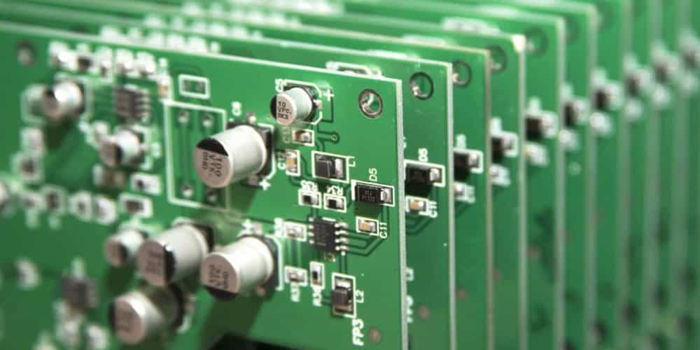
SMD or surface mount device is used in explaining the different electronic components that are utilized in and during the process of surface mount assembly. Out there, there are a whole lot of different packages for SMD components. Furthermore, you can find them in many different sizes and shapes
What is the Surface Mount Assembly Process?
Here, the surface mount technology (smt) process begins at your design phase. This is a time when you will select a whole lot of different surface mount components. Also, the design of the PCB is done with the help of software packages like Cadstar or Orcad. Note that there are others you can use.
It is very necessary that you note that the entire process of surface mount technology begins here. This is because it is the right time to integrate and incorporate a whole lot of design features. This will assist in straight forward and head-ache free production. Usually, the circuits can be taken or moved from its schematic design phase into the PCB layout. Here it will still have the functionality as the major considerations. This is very necessary, however the DFMA (design for manufacture and pcb assembly process ought to be integrated.
Immediately you are done with finalizing the PCB design and you have chosen the components, next is sending away the PCB data to your PCB manufacturing company. Next is purchasing the smt component leads suitably to help in facilitating automation. In addition, the design of the PCB panel has to be considered. Also, the specification has to be created with the PCB surface finish. This ensures that the PCB’s format is received as expected and also works for the use of the machines.
How are the components packaged?
The available components are usually packaged in different ways. This can be in trays, in tubes, in reels, as seen below. Furthermore, the majority can be seen on reels. This is much preferred. However, at times, as a result of the MOQs (‘Minimum Order Quantities) the supply of these components are usually done in tubes as well as short tape strips.
Also, these two packaging are useful, but they require the appropriate or right feeder types. Furthermore, the components that are supplied very loose in the bags have to be avoided as much as possible. This is because it can result in hand placements as well as the need to have special feeding plates. Note that all the components having a moisture sensitive level (MSL) must be handled adhering to the J-STD-033.
Machine programming
Once gotten the PCB components and PCB panels, then you can go ahead with setting up the different machines. This will be useful in the entire manufacturing process. These machines include the Automated Optical Inspection (AOI) and placement machine may need to create a program that is generated best from the CAD data. However, one issue here is that it isn’t usually available.
Furthermore, the Gerber data is usually available. This is because it is the main data needed for the manufacturing of the bare PCB. Also, if the Gerber data becomes the only available data then creating the CPL file (component placement list file) and centroid or the XY file could take so much time (time consuming). Therefore, the surface mount process usually offers this service to help in generating this file. Now, let’s go to the next step, which is the solder paste printing.
Solder Paste Printing
When setting up during the manufacturing process, the first ever machine to use will be the solder paste printer. This printer is designed to help with the application of the solder paste making use of squeegees and a stencil to the right and appropriate tool called solder pads present on the printed circuit board (PCB).
The method here is the one widely used for the application of the solder paste. However, for jet printing, it is now becoming very popular, most especially for the sub-contract sector. This is because you don’t need stencils and it is easier to make modifications.
It is very important when you keep control of the entire process. This is because if there is a printing defect left undetected, you will experience more defects as you continue with the manufacturing process. Also, as assemblies are becoming much more complex, your stencil’s design is important and you must take care to ensure that the entire process is stable and repeatable.
Solder Paste Inspection (SPI)
Majority of machines for solder paste printing usually include the option of automatic inspection. However, this depends on the PCB size, as the entire process could be very time consuming, and then a different machine could be preferred. These inspection systems in the solder paste printers make use of the 2D technology while the SPI machines make use of the 3D technology in enabling an inspection that is more thorough, which includes the volume of the solder paste for each pad and not the print area alone.
Component Placement
Immediately you have confirmed the printed PCB to include the right solder paste amount applied, the then next thing is moving it in the next stage of the entire manufacturing process – the component placement.
Every component is chosen for the packaging, making use of either gripper nozzle or a vacuum. This is then checked with the help of the vision system, and then you place it in that programmed location and at a very high speed.
In addition, there are different machines that will help achieve the process. This greatly depends on the business as well as the machine type chosen. For instance, when you focus the business around huge build quantities, you will discover that its placement rate becomes very important. However, when the focus is on high mix/small batch then the flexibility becomes more important.
To make sure that there is a repeatable and accurate component placement, you must know that you must support the populated PCB completely- The support systems of the PCB are revealed here.
Automated Optical Inspection (AOI) – Pre-Reflow
After the process of component placement, there is a need to confirm that there are no mistakes. Also, you must note that you have correctly placed all the parts before you continue with reflow soldering. One great way of achieving this is making use of the AOI machine. This conducts checks like polarity, value/type, and component presence.
First Article Inspection (FAI)
Verifying the first assembly is a well-known challenge for different sub-contract. Another challenge is the first article inspection (FAI); this is because it could be time consuming. Also, this step is very important in the entire process as the undetected errors could cause you to have much rework.
Reflow Soldering
Immediately you have checked all the component placements, you can then move the PCB assembly process into your reflow soldering machine. This is where the formation of the entire electrical solder connections is done between the PCB and its components by heating it to reach a sufficient temperature.
Also, this appears to become a less complicated part of the entire assembly processes and reflow soldering. However, the right reflow profile is important in ensuring solder joints that are acceptable without bringing any damage to the pcb assembly process and its parts as a result of excessive heat.
When making lead-free solder, it becomes very important to use a well-profiled assembly. This is because the temperature could become too close to the highest rated temperature of the many components
Automated Optical Inspection (AOI) – Post Reflow Process
The final part of your surface mount assembly process involves checking again to be sure that there are no errors or mistakes that could have happened when making use of the AOI machine in checking the solder joint quality.
Furthermore, introducing the 3D technology, the process becomes much more reliable like that of the 2D inspection, it reveals many false calls while interpreting the 2D image. Furthermore, with 3D inspection, accurate measurements have been taken and an inspection process that is more stable has been provided.
Another new feature of inspection machines, which you can network together to ensure instant feedback, which in turn enables automatic adjustments. For instance, you can connect your AOI machine to your placement machine ensuring that you can adjust the positions of the component placement and you can connect the SPI machine to your printer to permit adjustments when aligning the PCB to the stencil.
Through-hole Assembly
This is also selective soldering. Though selective soldering forms an aspect of through-hole assembly, there are so many areas, which affects PCB design and surface mount assembly like component position.
Designing your PCB while noting how you want it assembled will ensure labor cost savings as well as assembly lead time. Also, you will notice an improvement in the FPY (first pass yield). This will happen by the automation of many processes.
Process Verification making use of X-Ray Inspection
As a result of many hidden solder joints, it is very important that you possess a non-destructive inspection method used in verifying the whole soldering processes as well as delivering the best and desired results.
With X-ray inspection, it allows you to check the underneath components like voiding amount present in the solder joints and BGAs. Also, you can use it in verifying the fill of the solder hole after the soldering process
The Hand Soldering of the Surface Mount Components to the IPC Class 3
The fitting and soldering the surface mount components automatically is preferable. Though, at times, it is very necessary and important to hand fit it and solder. Now, this could become an issue with some components that have extremely delicate leads. Moreover with expert practice and specialist knowledge, it becomes possible.
Increase in Productivity and Efficiency
A very shocking statistic reveals that in the electronic industry, a lot of surface mount operations. This holds most especially in the sector of sub-contract manufacturing, running at about 20% efficiency. Also, so many reasons exist, which contributes to the figure. However, this fundamentally indicates that just 20% of this capital investment has been used.
Speaking financially, this leads to high ownership cost as well as slower returns on investments. For customers, this could result in longer lead times, therefore preventing the competitiveness of the business in the market.
Furthermore, when there are efficiencies in production for this particular level, This leads to some things. These include a lot of knock-off effects, which can affect the business like more batch sizes. Also, there will be more work in progress assembles, more parts readily available, as well as slow reaction times to the change requirements of the customer.
Knowing this, there will be a very strong incentive in improving efficiency as well as maintaining quality.
Conclusion
Surface mount technology assembly or SMT assembly line is a very significant aspect of electronic assembly. It is useful in the mounting of electronic components and smt components onto the printed circuit board (PCB) surface.
