Table of Contents
ToggleDesigning an AC to DC converter PCB layout can be a challenging task for even the most experienced engineer. The converter’s performance, efficiency, and reliability are all heavily dependent on the layout design. Therefore, it is crucial to pay close attention to the layout’s details to ensure the converter’s optimal performance.
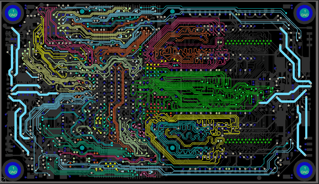
One of the key considerations in designing an AC to DC converter PCB layout is the component placement. The placement of components can significantly affect the converter’s performance, especially in terms of noise and heat dissipation. Additionally, the placement of components affects the converter’s size, which can be an essential factor in some applications. Therefore, it is crucial to carefully consider the component placement to ensure the converter’s optimal performance and size.
Another critical factor in designing an AC to DC converter PCB layout is the routing of the power and ground planes. The routing of these planes can significantly affect the converter’s noise performance and its ability to handle high currents. Therefore, it is essential to ensure that the power and ground planes are routed correctly to minimize noise and maximize the converter’s performance.

Basic Principles
AC to DC Conversion
An AC to DC converter is an electrical circuit that converts alternating current (AC) to direct current (DC). This conversion is necessary for many electronic devices that require DC power to operate. The conversion process involves rectification and filtering of the AC signal. The rectification process converts the AC signal to a pulsating DC signal, while the filtering process smooths out the pulsations to produce a steady DC voltage.
There are two types of rectifiers: half-wave and full-wave. A half-wave rectifier allows only one half of the AC signal to pass through, while a full-wave rectifier allows both halves to pass through. Full-wave rectifiers are more efficient than half-wave rectifiers, and they produce a smoother DC output.
PCB Design Considerations
The design of the PCB layout for an AC to DC converter is critical to its performance and reliability. The layout should be designed to minimize noise, reduce heat, and provide adequate spacing between components to prevent electrical interference.
Some of the key design considerations for an AC to DC converter PCB layout include:
-
Component placement: Components should be placed in a way that minimizes the length of the traces between them. This reduces the likelihood of noise and interference.
-
Trace width: The width of the traces should be adequate to carry the required current without overheating. The thickness of the copper layer should also be considered.
-
Ground plane: A solid ground plane should be used to provide a low-impedance path for the return current. This helps reduce noise and interference.
-
Heat dissipation: Components that generate heat, such as diodes and voltage regulators, should be placed in areas with good airflow. Heat sinks and thermal vias can also be used to dissipate heat.
-
EMI shielding: Shielding can be used to prevent electromagnetic interference from affecting the circuit.
In conclusion, designing a PCB layout for an AC to DC converter requires careful consideration of various factors, including component placement, trace width, ground plane, heat dissipation, and EMI shielding. By following these design considerations, the AC to DC converter can operate efficiently and reliably.
Components

When designing an AC to DC converter PCB layout, it is important to choose the right components to ensure proper functionality and efficiency. The following are some of the key components that are commonly used in AC to DC converter PCB layouts.
Diodes
Diodes are essential components in AC to DC converter PCB layouts. They are used to convert AC to DC by allowing current to flow in only one direction. The most commonly used diodes in AC to DC converters are rectifier diodes, which are designed to handle high currents and voltages. Schottky diodes are also used in some AC to DC converter PCB layouts due to their low forward voltage drop and fast switching speed.
Capacitors
Capacitors are another important component in AC to DC converter PCB layouts. They are used to filter out AC ripple voltage and provide stable DC output voltage. Electrolytic capacitors are commonly used in AC to DC converter PCB layouts due to their high capacitance values and low cost. Ceramic capacitors are also used in some AC to DC converter PCB layouts due to their low ESR and high frequency response.
Transformers
Transformers are used in AC to DC converter PCB layouts to step down the AC input voltage to a lower voltage that can be rectified and filtered to provide DC output voltage. The most commonly used transformers in AC to DC converter PCB layouts are center-tapped transformers, which have a center tap on the secondary winding that provides a reference point for the rectifier diodes. Toroidal transformers are also used in some AC to DC converter PCB layouts due to their compact size and high efficiency.
In summary, diodes, capacitors, and transformers are key components in AC to DC converter PCB layouts. Choosing the right components can ensure proper functionality and efficiency of the converter.
Layout Design
When designing an AC to DC converter PCB layout, it is important to consider the placement of components, trace routing, grounding, and shielding to ensure optimal performance and reliability.
Placement of Components
The placement of components on the PCB should be carefully considered to minimize noise and interference. Components should be placed in a logical and organized manner to ensure efficient current flow and minimize signal loss.
Trace Routing
Trace routing is crucial in an AC to DC converter design as it can impact the efficiency and stability of the circuit. Traces should be kept as short as possible to minimize resistance and inductance. Additionally, traces carrying high-frequency signals should be routed away from traces carrying low-frequency signals to avoid interference.
Grounding
Proper grounding is essential for the stability and performance of an AC to DC converter. A solid ground plane should be used to provide a low-impedance path for current flow and to minimize noise and interference. Ground traces should be kept separate from signal traces to avoid crosstalk.
Shielding
Shielding is an effective way to reduce electromagnetic interference (EMI) in an AC to DC converter design. Shielding can be achieved by placing a conductive shield around sensitive components or by using a grounded copper pour on the PCB.
In summary, a well-designed AC to DC converter PCB layout should consider the placement of components, trace routing, grounding, and shielding to ensure optimal performance and reliability.
Testing and Troubleshooting

Testing Procedures
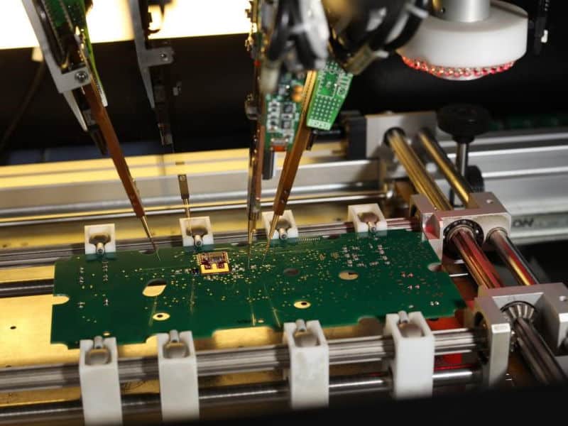
Once the AC to DC converter PCB layout is complete, it’s important to test it thoroughly before putting it into operation. The following procedures can be used to test the circuit:
- Check the input voltage with a multimeter to ensure that it matches the rated input voltage of the converter.
- Connect a load to the output of the converter and measure the output voltage with a multimeter. The output voltage should be within the specified range.
- Measure the ripple voltage using an oscilloscope. The ripple voltage should be within the specified range.
- Measure the efficiency of the converter using a power meter. The efficiency should be within the specified range.
Common Issues and Solutions
Despite thorough testing, issues may still arise with the AC to DC converter. Some common issues and their solutions are:
- Overheating: If the converter is overheating, it may be due to insufficient cooling or a faulty component. Check the cooling system and replace any faulty components.
- Output voltage fluctuations: If the output voltage is fluctuating, it may be due to a faulty capacitor or inductor. Check these components and replace them if necessary.
- No output voltage: If there is no output voltage, it may be due to a blown fuse or a faulty rectifier. Check these components and replace them if necessary.
- Overloading: If the converter is overloaded, it may be due to a load that is too heavy for the converter. Reduce the load or use a more powerful converter.
By following these testing procedures and addressing common issues, the AC to DC converter can be successfully implemented in a variety of applications.

