PCB Project Dynamics and Enhancement
We can use PCB (Printed Circuit Board) boards to build a circuit and program microcontrollers, but they can also design and print your project boards. It’s not difficult, but it does require some soldering skills and instruments that you may not have access to. Many websites offer free or low-priced PCB board services that will help you do most of the work for you with just a few clicks. It’s a great way to save some money and still get your hands dirty and make something with your own hands (and mind).
There are many types of PCB boards. But, the most common types people work with today are perfboard or Veroboard, single-sided PCB board, and double-sided PCB board. These will be the focus of this article.
Perfboard
Perfboard (also known as Veroboard) is a little like woodworking for engineers. Many integrated circuits (ICs) form a grid of copper traces on both sides of a polymer (plastic) base sheet. Designer lay out the IC on wood or “board” like material, like card stock, 0.010″ thick, on which one cuts 0.025″ thick sheets for each IC one will be mounting on the board.
Many online services will do this for you for low prices (e.g., PCBonino, ePCMaschinen). The most common circuits built on perfboard are hobbyist ones. But sometimes, you’ll find professional engineers use them—a typical Veroboard layout. A precise layout is not necessary with Veroboard, but at least try to make everything conform to the board’s shape.
Request PCB Project Quote, Pls Send PCB Files to Sales@raypcb.com Now
Single-sided PCB boards
Single-sided PCB boards are pretty much the same as perfboard, except they have copper traces only on one side. You can coat the other side with a non-conductive or insulating material. They include polyimide, paper, fiberglass cloth, or other substances. The traces are generally 1/4 to 1/2 oz. Copper and spaced between 0.010 and 0.025″ apart.
It’s also common for single-sided PCB boards to have ground planes and power planes on one or both sides. They help reduce EMI and RFI interference and common mode noise issues. These are usually a product of copper foil and the other traces on each side of the board. Single-sided PCB boards are commonly valuable for hobbyist projects and commercial products—a typical single-sided PCB layout. A precise layout is not necessary with a single-sided PCB, but try to make everything conform to the board’s shape.
Double-sided PCB boards
Double-sided PCB boards are like single-sided ones, except there are traces on both sides. It’s obvious how the traces are evident.
A typical double-sided PCB layout. A precise layout is unnecessary with a double-sided PCB, but at least try to make everything conform to the board’s shape.
Anyone can order the Double-sided PCB boards through many online services, such as OSH Park (recommended), BatchPcb, and others. These services have an excellent user interface and will do the layout for you automatically.
What is a PCB project?
You can build a circuit board by laying out the circuit or program on your perfboard, single-sided PCB board, or double-sided PCB board. It’s like the electronic equivalent of an artist’s canvas (the board) you paint (layout the circuit or program). The only difference is that you need to do some wiring before painting. It is a great way to learn about electronics and circuits. But, it’s also a great way to design prototypes for your inventions, no matter how small or complicated.
Why use the PCB project?
It’s a great way to essentially design circuits on the fly. You can make circuit designs, typically laid out on perfboard, single-sided PCB board, or double-sided PCB board. Then transfer them to your circuit board projects. It’s also a great way to experiment with different circuit designs without investing too much money in equipment that may not last long.
Can you make PCB at home?
Yes. You can build your own circuit board at home if you have the right equipment and skills. It is a great way to make prototypes; however, it may cost more than buying one from an online service such as OSH Park.
You can create your PCB by ordering pre-sensitized boards from OSH Park or other online services. You will need to order 1,000 of them because they only make the boards in lots of one thousand. But, since they are individual boards, you can use them as-is for single-sided PCB board projects. You can also break them up into smaller stacks of 500 to make double-sided PCB board projects.
You can also create your PCB by using the software-defined radio (SDR) software-defined radio (SDR) software. These are pieces of software that allow you to build your custom radios from scratch with a computer and soldering equipment.
How to build a PCB project?
You’ll need to use soldering equipment to solder the components to your PCB construction. If you are using a perfboard, single-sided PCB board, or double-sided PCB board, you’ll have to wire up all the components before you can test them. The best way is to put each component where you will mount it on your PCB project.
Check to see that everything fits, then test. If it all works, you are close to completion. It’s also a good idea to make sure that each of the components has a dedicated ground. You can solder them with the same color of solder that they are on your PCB project since green is the most common ground color for many components.
Double-side PCB boards can be hard to use if you don’t have access to the proper tools and equipment. You can get schematics of the circuit and components on the board, but you’ll need to add them to your PCB project layout. Many online services such as Hackaday, Oscillocast, and others offer free PCB layouts for DIY projects.
What are the characteristics of a good PCB design?
There are all sorts of things that go into the PCB design projects, but here are some of the most important characteristics.
It should be versatile enough to support many different types of applications
If you are building a custom circuit board, try to design it without limitations on one type of application. There may be reasons why you want to do this. Such as if you will sell the product in stores and need it to remain generic so that other people can use it for their applications or modifications. Consider the types of applications and plans you will use with your circuit or program and ensure they will work correctly
It should be easy to read, understand, and follow
When creating your PCB design, you can do many different things to make it rather complicated. Such as making it very detailed with lots of unique numbering and symbols for each component. Also, there can be a lot of space on the board not used for anything. Would you mind keeping all your PCB design in a way that makes them easy to follow? You can do it by using a simple numbering and symbol system and mostly using the space to make sense.
It should be easy to make changes to it when they are necessary
As you create your PCB design, you may find problems or areas of your project that you need to modify slightly. It doesn’t mean you have to start from scratch if they aren’t too complex
It should be easy to assemble
As you design your PCB project, consider how it will go together when you finish. Will you have to solder all the components by hand? Can you buy a pre-assembled panel? Will there be one or more ‘dummy’ boards with connectors so that you can easily connect everything up to test things out before putting it all on your finished board? Consider what you need when building your circuit and add these extra components in if you need them.
Request PCB Project Quote, Pls Send PCB Files to Sales@raypcb.com Now
It should be easy to test out with a multimeter
It is essential to test things out before putting them on your finished PCB project. Even if you do nothing special with the circuit, you should still test it out before mounting it on your finished PCB project. It helps ensure that there are no electronic shorts or other mistakes in your wiring that could damage the components or even fry them.
It should be able to handle voltages that may exceed recommended limits without damage
Suppose you use specific components such as MOSFETS, transistors, or any other electrical component that does not have built-in over-voltage protection that limits their voltage. In that case, you must use a rated circuit to support these higher voltages without damaging them.
It should handle the temperatures and stresses of normal and high usage without damage
A great way to test a circuit is to use it as you usually would. It will help you see how it handles the different amounts of current draw and temperature changes without damage. You can do it by using a multimeter to measure the current draw of your circuit while it is under normal use. Then using a combination of a digital thermometer and a hygrometer to test out how well your circuit handled those stresses.
You should design it with some protection for all components
Even the best circuit board projects will have failure or problems with them during their use. It can be from a poorly soldered connection, a short circuit, or other problems that may damage the components. As you start to design your PCB project, try to think of how it could fail. Include a ‘failsafe’ design so that there is no permanent damage to any of the components if a connection breaks apart.
It should be easy to change by expansion later
If you make your PCB project in a way that allows for extra spots in the design, you can easily add new parts to it later. For example, make a custom circuit board for an RC car’s motor controller. You could leave plenty of connectors available so that you could easily add in extra sensors or features to it later without having to mess with the original design.
It should be easy to build by hand
It is almost inevitable that you will have to build at least a few of your PCB projects by hand. Suppose you make a circuit board project complicated enough for this to be a problem. You will have a hard time going from the design to the finished product without spending much money or time on it. Find a balance between what components and features you need and the ease of building it by hand.
PCB projects for beginners
We use it in most modern electronic devices. They help provide communications between the electronic components on the PCB and other electronic devices attached to this PCB (i.e., a computer). A small printed circuit board can provide a simple way to implement a circuit for the individual building a circuit for personal use.
To create a PCB, there are two main steps. First, you must create the circuit design in an appropriate computer program. Then, after exporting to a file format readable by a PCB manufacturer’s software or equipment, it sends the file to a fabrication facility to create the desired PCBs.
PCBs can contain several layers of copper interconnections. For a given circuit, one interconnection can be straight between components of a device. For example, the resistor might have a straight connection to a power supply or ground terminal from one of its legs. An inductor might have a straight connection from the loop to the input or output terminals of the device.
A capacitor could have a straight connection from one end to another end. Each component has special needs in terms of electrical characteristics. They also must relate to other similarly-capacitor components designed for relatively specific characteristics. A particular capacitor needs a capacitor with the required capacitance—a resistor that has a resistance that matches the desired range of resistance, and so on. You must make a connection from one end of the device to another in a specific connection scheme.
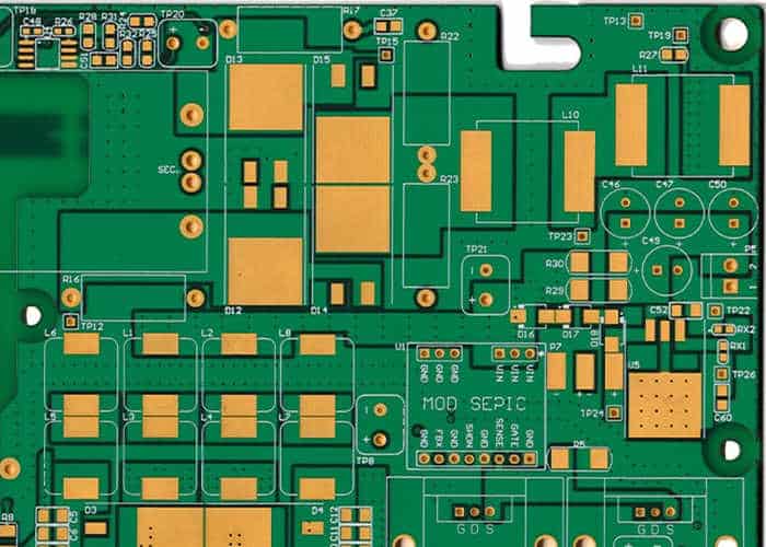
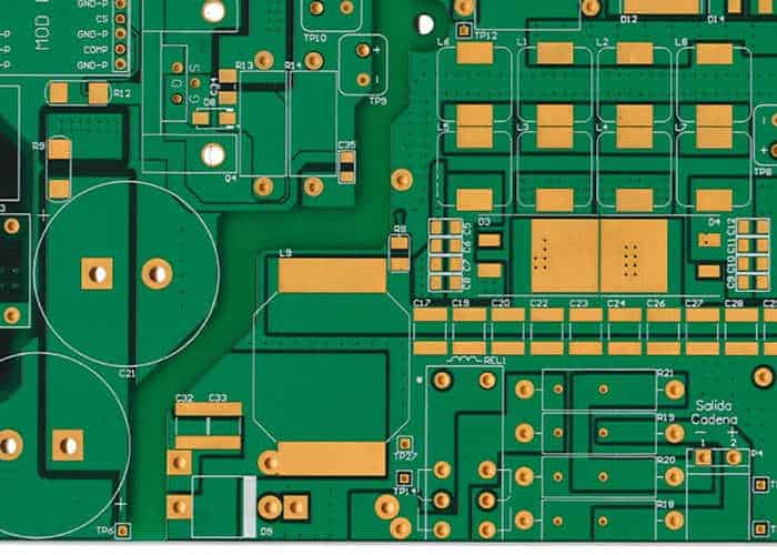
PCB layers
A PCB comprises many layers of copper interconnections. You can cut each layer with tools such as lasers and water jets. We refer to the copper layers fixed together as “plated-thru” or “tinned-thru.” “Tinned-thru” refers to a process by which we first solder the component leads to the copper pads on one side of the board. Then we apply a second tin coating onto those connections on the other side of the PCB that we will use to connect to another layer.
One can make PCBs with several layers. You can also separate the layers by insulating sheets, such as fiberglass, Kapton, or FR4. Each of these insulating sheets has characteristics that are useful for certain types of applications.
One can match the layers using special fixtures that pick up the board coated in the photoresist and then place it onto the next copper layer. We can move the board around using robotics to align each layer with one another. We cure the copper and photoresist used, placing the next layer of copper and more circuit design onto the board.
Once you complete the assembly of layers, we use a red laser to cut all the layers together. It allows for easier handling of the finished product and more accurate cuts than water jets. We then apply a sheet such as fiberglass over each copper layer. The fiberglass acts as temporary insulation before the actual PCB assembly. Once you assemble the copper layers, you cover everything in a tin binder, leaving all the insulation.
PCB Assembly
Typical assembly time takes several hours to complete depending on where in the world it is being done. You then inspect the printed circuit boards by a machine that sorts through any workmanship defects or materials.
There are several methods to create your very own custom printed circuit board. To purchase a PCB from a manufacturer, you will need to contact the manufacturer and request the design for your project. In most cases, it is possible to produce a custom PCB without contacting a PCB manufacturer. Still, you will have to find someone who has access to the PCB software and the equipment necessary for creating a custom PCB.
Creating custom PCBs
The process of creating a custom printed circuit board starts with downloading a design from an appropriate website. The design will probably have to be in a PDF or graphically based format, but not always. We can export it directly to a PCB manufacturer’s software or an LQDD. You can also design the PCB using an appropriate PCB design program. Export it to PCBasic, or export it to another CAD program.PCB, Freepcb, KiCad, PepcoBoard, or Altium Designer and import it into PCBasic.
Once you import the design into PCBasic, It represents the board in the drawing section. The next step in designing a custom printed circuit board is to add components to the design. Several components are essentially must-haves for any PCB. They include power distribution components, resistors, capacitors, inductors, and ICs.
Request PCB Project Quote, Pls Send PCB Files to Sales@raypcb.com Now
Adding component value to your PCB design
There are several approaches for adding component values to your PCB design. Some software programs offer an “auto-populate” function that will populate proper values for all components. Some software programs such as PepcoBoard and PepcoCAD do not include this function.
You can use a text editor to enter each component value manually. While this is an option, the actual process of entering component values and placing them in the proper position in the design can be time-consuming and tedious. Once you finish your design, you will need to export it to a PCB manufacturer’s software or laser cutter. You must cut each layer of your design individually before moving on to the next layer. PCBasic will generate an error if not cut the design layer-by-layer or if layers are not cut in the correct order.
Final fabrication
The final step in creating a custom printed circuit board is to fabricate by getting it laser-cut out of copper sheets. It creates a finished product that you can then assemble into your final project.
There are many ways to create your custom printed circuit board, each has its own merits and demerits, so it is up to you which method you use. Creating your custom printed circuit board is a popular way to get exactly what you want. Working with leading manufacturer like RayMing PCB and Assembly, will help you get the best designs and products.
Advantages of PCB projects
Affordable
With the advances in technology, manufacturing costs have significantly decreased. With the advent of robotics and 3-D printing, it is now possible to produce a custom printed circuit board. You can do it for a fraction of what it would have cost just a few years ago. As prices continue to drop, there is no reason that cheap custom printed circuit boards will not soon be affordable to everyone who wishes to use them for their project.
Speed
In today’s world, speed is of the essence. You can significantly reduce the time to produce a custom printed circuit board with modern manufacturing techniques. Besides having custom-printed circuit boards quickly, you can also produce them in large quantities at a reasonable price.
No minimum order quantity. PCB project has no minimum order quantity. While it is easier and faster to produce a smaller quantity of PCBs, you can always do this if you need just one PCB.
Flexibility
With modern manufacturing techniques and methods, it is now possible to produce a single custom printed circuit board for a design or several boards with the same design. It allows you to develop a design and get many different variations to choose from. You can finally create something that fits your needs perfectly. With the freedom of creating what you want comes freedom.
Higher quality
The manufacturers of custom printed circuit boards can produce a much higher quality product. The techniques used allow for a better result in a shorter time, reducing errors and inconsistencies. In addition, the manufacturing processes are more efficient, allowing for lower costs per piece. PCBWay can produce custom printed circuit boards at extremely low prices to sell them at the lowest possible price.
Conclusion
In conclusion, creating your custom printed circuit board is an excellent investment in your project and your future. Since you have the freedom to create exactly what you want, you can take your project to a whole new level.
