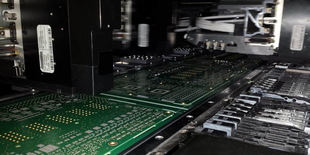
Additive PCB manufacturing is a process that is gaining popularity in the electronics industry. This method of manufacturing involves adding material layer by layer to create a circuit board, as opposed to traditional methods that require the removal of material.
One of the main advantages of additive PCB manufacturing is that it allows for greater design flexibility. With traditional methods, designers are limited by the tools and equipment available to them. However, with additive manufacturing, designers can create complex shapes and structures that would be difficult or impossible to achieve with traditional methods.
Another advantage of additive PCB manufacturing is that it can be more environmentally friendly than traditional methods. Traditional methods often involve the use of harsh chemicals and generate a significant amount of waste. Additive manufacturing, on the other hand, can use materials that are more environmentally friendly and generate less waste.
Advantages of Additive PCB Manufacturing
Additive PCB manufacturing, also known as 3D printing, is a newer technique that has gained popularity in recent years. This manufacturing process involves building up layers of material to create a three-dimensional object. In the case of PCB manufacturing, this means printing the circuit board layer by layer. There are several advantages to using additive PCB manufacturing over traditional manufacturing methods.
Cost Efficiency
Additive PCB manufacturing can be more cost-efficient than traditional manufacturing methods because it requires less material and labor. Traditional manufacturing methods involve cutting and etching copper sheets to create the circuit board, which can be time-consuming and wasteful. Additive manufacturing only uses the amount of material needed to create the circuit board, reducing waste and saving money. Additionally, 3D printing can be done in-house, eliminating the need to outsource the manufacturing process.
Design Flexibility
Additive PCB manufacturing allows for greater design flexibility than traditional manufacturing methods. With 3D printing, designers can create complex shapes and designs that would be difficult or impossible to achieve with traditional methods. This allows for more creativity and innovation in PCB design, which can lead to better-performing and more efficient circuit boards.
Reduced Waste
Additive PCB manufacturing produces less waste than traditional manufacturing methods. Because the circuit board is printed layer by layer, only the necessary amount of material is used. This reduces the amount of waste generated and makes the manufacturing process more environmentally friendly. Additionally, any leftover material can be recycled, further reducing waste.
In summary, additive PCB manufacturing offers several advantages over traditional manufacturing methods. It is cost-efficient, allows for greater design flexibility, and produces less waste. As 3D printing technology continues to advance, it is likely that additive PCB manufacturing will become even more popular in the future.
Challenges of Additive PCB Manufacturing

Limited Material Selection
One of the biggest challenges of additive PCB manufacturing is the limited material selection. Unlike traditional PCB manufacturing, which can use a wide range of materials, additive manufacturing is limited to a few specific materials. Currently, the most commonly used materials for additive PCB manufacturing are copper and silver. While these materials are suitable for many applications, they may not be suitable for all.
Surface Finish Issues
Another challenge of additive PCB manufacturing is surface finish issues. Additive manufacturing techniques can result in rough surfaces that may not be suitable for some applications. Surface finish is important for many reasons, including electrical conductivity, corrosion resistance, and aesthetics. While some additive manufacturing techniques can produce smooth surfaces, others may require additional processing to achieve the desired surface finish.
In conclusion, additive PCB manufacturing offers many benefits, including reduced waste, faster turnaround times, and greater design flexibility. However, it also presents some challenges, such as limited material selection and surface finish issues. As the technology continues to evolve, it is likely that these challenges will be addressed, and additive PCB manufacturing will become an even more viable option for PCB production.
Comparison with Traditional PCB Manufacturing
Differences in Process
Additive PCB manufacturing is a relatively new process that differs from traditional PCB manufacturing. In traditional PCB manufacturing, a subtractive process is used, which involves etching away copper from a copper-clad substrate to create the desired circuit pattern. On the other hand, additive PCB manufacturing involves the deposition of copper onto a substrate to create the circuit pattern.
In the subtractive process, a substrate is coated with a layer of copper, and a photoresist is applied to the copper layer. The photoresist is then exposed to light through a mask, which causes the resist to harden in the areas where the circuit pattern is desired. The unhardened areas are then etched away, leaving behind the desired circuit pattern. In additive PCB manufacturing, the substrate is coated with a thin layer of copper, and the circuit pattern is created by selectively depositing additional layers of copper onto the substrate.
Quality Comparison
Additive PCB manufacturing offers several advantages over traditional PCB manufacturing in terms of quality. First, additive manufacturing allows for the creation of more complex circuit patterns, including those with finer features and tighter tolerances. This is because the additive process allows for the precise deposition of copper onto the substrate, whereas the subtractive process can result in over-etching or under-etching of the copper.
Second, additive PCB manufacturing can result in a more uniform copper thickness across the substrate, which can improve the overall performance of the circuit. In traditional PCB manufacturing, the etching process can result in variations in the thickness of the copper, which can affect the electrical properties of the circuit.
Finally, additive PCB manufacturing can reduce waste and environmental impact compared to traditional PCB manufacturing. The subtractive process can result in the generation of hazardous waste, including chemicals used in the etching process. In contrast, additive PCB manufacturing does not require the use of these chemicals and can result in less waste overall.
Overall, additive PCB manufacturing offers several advantages over traditional PCB manufacturing, including the ability to create more complex circuit patterns, improved uniformity of copper thickness, and reduced waste and environmental impact.
Future of Additive PCB Manufacturing
Additive PCB manufacturing has opened up new possibilities in the electronics industry. While traditional subtractive methods are still widely used, additive manufacturing is quickly gaining ground. The future looks bright for additive PCB manufacturing, with several advancements expected in the coming years.
Advancements in Materials
One of the major advancements expected in additive PCB manufacturing is the development of new materials. Currently, most additive PCBs are made using conductive ink or paste. However, researchers are working on developing new materials, such as graphene, that will allow for even smaller and more complex circuits.
Increased Automation
Automation is another area where additive PCB manufacturing is expected to see significant advancements. Currently, the process of creating an additive PCB requires a lot of manual labor. However, with the development of more advanced machines and software, it is expected that the process will become more automated, reducing the need for human intervention.
Customization
Additive PCB manufacturing is already allowing for greater customization in the electronics industry. However, with advancements in software and automation, it is expected that this customization will become even more prevalent. This will allow for greater flexibility in design and production, allowing companies to create products that better meet the needs of their customers.
Overall, the future of additive PCB manufacturing looks bright. With advancements in materials, automation, and customization, this technology is expected to continue to grow and revolutionize the electronics industry.
