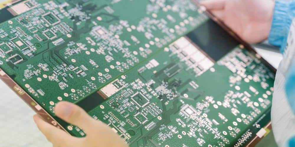
This is a process of producing electronic circuit boards. It uses two different types of ink. Clear-ink printing is used on the non-conductive outer layer of the PCB, while black-ink printing is ideal on the conductive copper layers. We then apply these inks to the PCB’s inner and outer layers.
PCB Printers
PCB printers can create multilayer circuits using a technology similar to inkjet printers. These printers spray ink in tiny droplets onto the surface of the printed circuit. They can print various materials on the circuit board, including insulating materials that can act as middle layers. This technology allows the production of multilayer PCBs, which were unthinkable in the past.
There are two types of PCB printers. Some use piezo or thermal inkjet heads, and those use piezo or X-Y plotter technology. Both types can print features from 10 microns to millimeters in size.
PCB conductive Inks and Printing
PCB Ink and printing have a close relationship, but they also require different techniques. For example, the viscosity of ink has a significant effect on printing accuracy. If the ink is too viscous, it may cause leaks or graphics to be serrated. An excellent way to reduce the viscosity of ink is to dilute it with a diluent.
PCB Ink and printing is a common prototyping method. The process can turn a PCB layout into working prototypes in minutes or hours. In addition, it can print on different materials, which increases design flexibility. This is especially useful for emerging technologies.
The dry film solder method has been used for a few years but has a low yield and is very expensive. As a result, the use of LPI solder mask ink for high-density, high-precision PCBs is slowly gaining popularity.
PCB Printers That Use an Inkjet Approach
Inkjet PCB printers use a unique process to create boards. Instead of a special paper, the printer dispenses conductive ink, which ultraviolet light or CFL cures. This process allows for multilayer PCB printing and can create up to four-layer boards.
A common Inkjet printer can print on copper-clad boards. The paper used to print on this material is parchment paper, allowing more light to pass through it. This method is suited for a variety of other applications.
Printed Circuit Boards design
PCBs have a variety of functions and should perform these functions within the space allotted to them. This is accomplished through computer-aided design systems (CAD) and special software, allowing designers to lay out a circuit pattern. The computer design software also outlines the position of holes, which become CNC drilling machines. These machines also work by applying solder paste to complete the manufacturing process.
Surface Mount Components
Surface mount components are electronic components mounted on a surface. They are smaller and faster to install on a PCB than traditional components with wire leads. IBM was the first to introduce SMT electronics, demonstrating how small they could be. Philips followed suit with a surface-mounted button device, but it took time to take off. As a result, Philips had only a 10% market share by 1986. IBM essentially pioneered the process and designed the majority of the required components.
PCB Printing Solder Paste
A PCB printing process can be more efficient if the solder paste is appropriately applied. The stencil’s size affects the amount of solder paste applied to the PCB. The stencil’s apertures should be small enough to allow at least three millimeters of separation per second. A too large stencil will not allow for enough separation and cause excessively high edges around deposits.
Printing solder paste comes in a wide variety of grades. Some are used for general assembly, while others are ideal for manufacturing specialized products. There are even industrial-scale solder pastes that are essential for production-scale assembly lines. Some are also available in smaller quantities, such as tubs and syringes. These are ideal for general rework and BGA rework areas, as well as for small prototype assembly.
Computer-aided design (CAD) software
Designing a PCB involves designing the layout of the components on the board. We can do this manually or with the use of CAD software. The design must be precise, keeping in mind space requirements and the shape of the device. This process can be complicated, but the software helps to make the process simpler.
Many electrical engineers use CAD software for their design needs. Computer-aided design (CAD) software packages offer different tools and features for designing and printing a PCB using a Gerber file. These software packages often include predefined blocks, Gerber files, and scripts for various applications. They also contain tools to design digital and analog integrated circuits and backplanes with the help of a Gerber file. In addition, these CAD software packages help to make architectural drawings.
Using a trace width calculator
A PCB trace width calculator is a helpful tool when designing and printing a PCB. This tool calculates a circuit board’s trace width, length, and current. It is based on the IPC 2221 standard and can calculate traces up to 35 Amps with a maximum trace width of 400 mils. It also includes a chart of a copper thickness (0.5 to 3 ounces per square foot) and a temperature increase of 10 to 100 degrees Celsius.
An Alternative Metal for PCB Traces
Copper is one of the most popular metals used in printed circuit board traces. It is a low-cost metal and has a high conductivity. It is also a good choice for traces because it is readily available. Nickel can make PCB traces. It is also an alternative metal to copper rivets. However, this metal is not as widely helpful in PCB traces as copper. In addition, nickel is not as easily available as copper rivets. It is also harder to replace the lead of a component in the PCB’s interior. However, some versions of the cordwood construction use soldered single-sided PCBs.
Using a schematic to design a PCB
There are many things to consider when using a schematic to design a PCB. First, ensuring the drawing is clear and includes all the necessary information is essential. For example, the schematic should consist of information about the product or company, part numbers, and revision numbers, and we should check the schematic for obvious errors.
We can write a schematic or computer-generated one. Still, it is essential to remember that the schematic will not account for the placement of electronic components and traces between them. It also does not include the ground planes important for signal integrity in a real PCB.
After validating the schematic, you can move on to the next step. The next step is to add labels to the symbols. These labels will appear on the finished printed circuit board. You can easily change these labels if you want to. This step will also allow you to make changes to the board shape.
Labeling a PCB
Labeling a PCB is an essential step in the manufacturing process. It allows manufacturers to minimize downtime and ensure full manufacturing traceability. A PCB label must come from a durable material resistant to high temperatures and chemical agents. A PCB label should also have a specialized surface coating to ensure crisp printing. A standard desktop laser printer should be able to print a PCB label.
While silk screens are not high resolution, a photo plotter can draw these labels with high resolution. Therefore, a 300-dpi printer is necessary. Then, print the labels on the PCB using high-quality paper and ink. Finally, using a photo plotter, choose a thick font that is easy to read.
Top 4 PCB Printers

When looking for a PCB printer, it is essential to consider your needs. There are several different types of printers, and choosing the right one can be difficult. This article will discuss Voltera V-one, Squink, Kyosha Circuits, and Camptech II Circuits.
Squink
The Squink PCB printer prints boards in a matter of minutes. This flexible PCB printer is perfect for prototype PCBs. It can print conductive and non-conductive circuits on Kapton or FR-4 film and can even print multilayered circuits. The printer uses computer vision algorithms and a Sitara processor to print circuits using conductive ink.
The Squink is a first-generation desktop PCB printer. It can print multilayer circuits, dispense flexible substrates, and pick up components from a PCB board. Using this printer is easy but requires some training. Before users can use Squink, they must take a written exam and pass a hands-on exam. If someone is not qualified to use the machine, they will receive a warning and be required to retrain.
Volterra V-one
When setting up a Voltera V-one PCB printer, there are a few basic things to remember. First, you should align the board properly before you begin printing. This includes making sure that the clamps and the probe don’t move the board once it’s clamped.
The Voltera V-One is an additive PCB printer that creates two-layer prototype boards. It uses silver-based conductive ink to print the circuit board. This printer supports both additive and conventional boards. It also has reflow and paste dispensers, making assembling a PCB easy and fast.
You can use the Voltera V-one with a variety of CAD programs. It supports Altium, KiCad, Mentor Graphics, and Cadence. It’s also compatible with Arduino and Uno and can print on various flexible films such as Kapton.
Camptech II Circuits
PCB fabrication services from Camptech II Circuits Inc. are available for the entire range of build quantities from prototypes to small to medium production and high-volume manufacturing.
They offer competitive pricing, excellent pre-sale support, and a wide range of PCB manufacturing services. For example, PCB printers can produce both rigid and flexible boards. They can also offer quick-turn prototype manufacturing and box-build assembly services.
Advanced Circuits is the third largest PCB manufacturer in the country and offers free PCB design software and file-check services. Advanced circuits offer services that ensure that your PCBs are error-free and work perfectly.
Kyosha Circuits
Kyosha Circuits is a manufacturer of single-sided and double-sided printed circuit boards. Its manufacturing plant is in the Pearl River Delta area of China. It also manufactures copper-clad laminates and inks for marking and coating boards.
