Printed Circuit boards are, without a doubt, a marvel of engineering. These tiny yet complex pieces of tech are a significant feature of most electronics you will find in the market today. You can find them in miniature electronics such as wristwatches and smart watches and larger electronics like Televisions. What’s more, PCBs come in varying prices, complexities, and qualities, making their production much trickier to handle. From single to double and multilayer PCBs, all these varieties require extra manufacturing attention. So how do PCB manufacturing companies carry out PCB production flawlessly to achieve the PCB you find in electronics today?
The PCB Production Process
The Different Types of PCBs produced using this Process
The PCB production process that we shall go through cater to the production of the following types of PCBs:
- Rigid-flexible or Rigid-flex Printed Circuit Boards
- Flexible or flex Printed Circuit Boards
- Rigid Printed Circuit Board
- Multilayer Printed Circuit Board
- Double layer Printed Circuit Board
- Single layer or Single Sided Printed Circuit Board
The Production Process – step by step
Etching or Patterning
The PCB production process’s first step is etching or patterning. In this process, technicians mostly add a good layer of copper components onto the surface of the Printed Circuit Board’s substrate material. The technicians can choose to add the copper layer on one side or on both sides of the substrate material, depending on how one uses the PCB.
The addition of a copper layer generates a blank PCB that has copper scattered everywhere on the board’s surface.
From this point, technicians then utilize specialized machinery to remove excess copper from the PCB using a method known as the subtractive method.
Photoengraving
In the photoengraving PCB production procedure, technicians utilize a photomask merged with special chemicals to remove or subtract the copper regions from the board’s substrate.
A PCB photoplotter is the particular machine one uses to generate the mask utilized in this procedure. The machine utilizes the blueprint design produced on a CAB Printed Circuit Board software.
However, sometimes technicians utilize low-resolution photomasks produced using a laser printer, but the latter is always better.
Lamination
Most PCBs encompass more than one layer (hence called multilayer PCBs). In addition, these PCBs include more than one trace layer or thin etched boards, bound together through a process known as lamination in the PCB production process.
Multilayer PCBs tend to be more complex, and they take more time to produce compared to single-layer PCBs.
Drilling
Each PCB layer needs to have the ability to connect to another layer. To ensure that all layers bear this ability, technicians take all PCB layers through a drilling process that sees all the layers get holes drilled into them. These holes are known technically as vias, and they are very crucial.
The drilling process requires excellent precision, so many manufacturers utilize specialized drilling machines that work autonomously. These unique machines are controlled by a computer program and NCD files (excellon files) which dictate the size and position of each hole in the PCB’s design.
Moreover, using controlled depth drilling, technicians can quickly drill a single layer on a multilayer PCB instead of drilling through all the board layers, which makes the board more effective. Technicians achieve controlled depth drilling by drilling individual layers or sheets of the Printed Circuit Board before lamination.
Types of Vias
Buried vias
If the vias only connect interior layers, these holes are known as buried vias.
Blind Vias
If the vias connect a PCB layer to an external surface, these holes are known as blind vias.
After the drilling process is done, the walls of the vias are then copper plated to generate plated through holes. Technicians then utilize these through holes to connect the conductive PCB layers.
Solder Plating
Solder plating or solder resist involves plating the lands or pads of a PCB that will have electronic components mounted onto them to allow efficient solderability. Technicians carry out this PCB production process because bare copper isn’t readily solderable. Therefore, copper requires the addition of a surface plate to aid in the soldering process.
Earlier on, technicians utilized tin-based lead to carry out solder platting. However, with the emergence of RoHS (Restriction of Hazardous Substances), technicians are now migrating to using safer components such as gold and nickel.
During the solder plating process, you can cover the areas that don’t require solder plating using a solder resist material. The solder-resist component acts like a solder mask helping technicians avoid bridging traces as this can cause short circuits.

Silkscreen
When technicians need to add visible information onto a circuit board, for example, a part number or a logo, they turn to silk screening. That is because silk screening is the process of applying text onto the external layer of a PCB.
If the space is sufficient, technicians can add in:
- Component designators
- Switch settings requirements
- Additional features to help out manufacturers in the assembly process
You should also note that red print refers to writing or silk screening only on one side of a PCB.
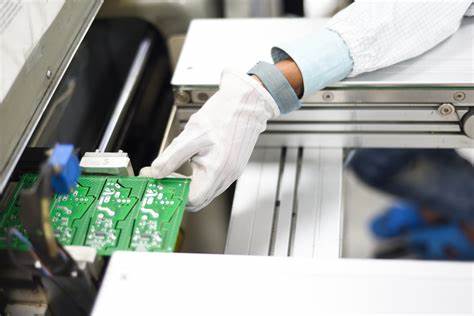
Testing
Printed Circuit Boards that are not assembled need to undergo a couple of checks to ensure that they function accordingly. During these tests, technicians verify that each circuit connection functions correctly.
When working with a high-volume circuit PCB, technicians use a fixture to connect to the holes, and copper lands on one or both sides of the PCB. These fixture helps facilitate faster and more efficient PCB tests.
Technicians also utilize computers to control electrical testing units, which boosts the precision and accuracy of the tests.
On the other hand, for small and medium volume PCB production tests, technicians utilize a flying probe tester which efficiently checks for electrical contacts. The flying probes utilized to carry out these tests use moving “heads” to touch the copper holes and lands. After making contact with these parts, the probes validate the board’s electrical connectivity.
Conclusion
Printed Circuit Boards have become a significant part of technological advancement. Through this technology, engineers have produced slim gadgets that perform or even outperform traditional devices that are pretty massive. However, the production process of these gadgets is not a simple task. Manufacturers must cycle through multiple stages to develop the perfectly functional PCB you find in most devices today. All the steps involved in the PCB production process are pretty necessary, and messing them up tends to breed bad outcomes.
