Common mode chokes are an essential component in electronic circuits that help to eliminate electromagnetic interference (EMI) issues. These chokes are used to suppress common mode noise, which is the noise that appears on both the signal and ground lines of a circuit. Common mode noise can cause various problems, such as signal distortion, decreased signal-to-noise ratio, and increased electromagnetic radiation.
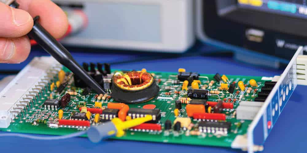
The layout of a common mode choke on a printed circuit board (PCB) is crucial for its proper functioning. The placement, orientation, and routing of the choke can significantly affect its performance. It is essential to keep the choke as close to the source of noise as possible and to avoid routing the signal and ground lines through the choke. Additionally, the orientation of the choke should be such that the magnetic fields produced by the current flowing through it cancel out the common mode noise. In this article, we will discuss in detail the various aspects of common mode choke PCB layout and provide guidelines for designing an effective layout.
What is a Common Mode Choke?
A common mode choke is an electronic component that is used to suppress electromagnetic interference (EMI) in electronic circuits. It is also known as a line filter or a signal filter. The choke is essentially a coil of wire that is wound around a magnetic core. It is designed to block high-frequency noise and unwanted signals while allowing the desired signals to pass through.
The common mode choke is used to suppress common mode noise, which is noise that appears on both the positive and negative lines of a circuit. This type of noise is caused by external sources such as power lines, motors, and other electronic devices. The choke works by creating a high impedance to the common mode noise, which effectively blocks it from entering the circuit.
The common mode choke is commonly used in power supplies, audio equipment, and other electronic devices that require high levels of noise suppression. It is particularly useful in circuits that are sensitive to noise, such as those used in medical equipment, aerospace applications, and telecommunications.
In summary, the common mode choke is a simple but effective component that is used to suppress unwanted noise and interference in electronic circuits. It is an essential part of any circuit design that requires high levels of noise suppression and signal integrity.
Why is PCB Layout Important for Common Mode Chokes?
Minimizing Parasitic Capacitance
The parasitic capacitance of a common mode choke can have a significant impact on its performance. Parasitic capacitance can cause the choke to resonate at frequencies other than the intended frequency, reducing its effectiveness. To minimize parasitic capacitance, it is important to keep the distance between the windings as small as possible. This can be achieved by using a PCB layout that places the windings close together.
Optimizing Placement
The placement of the common mode choke on the PCB can also have a significant impact on its performance. Placing the choke as close as possible to the source of the noise can help to reduce the amount of noise that is coupled into the circuit. It is also important to place the choke in a location that is free from other sources of electromagnetic interference (EMI), such as switching power supplies or high-speed digital circuits.
Routing
The routing of the traces on the PCB can also have an impact on the performance of the common mode choke. It is important to route the traces in a way that minimizes the amount of noise that is coupled into the circuit. This can be achieved by using a ground plane or by routing the traces in a way that minimizes their length and proximity to other sources of EMI.
In summary, the PCB layout is an important consideration when designing a circuit that uses common mode chokes. By minimizing parasitic capacitance, optimizing placement, and carefully routing the traces on the PCB, it is possible to maximize the effectiveness of the common mode choke and reduce the amount of noise that is coupled into the circuit.
Best Practices for Common Mode Choke PCB Layout

Keep Traces Short and Direct
When designing a PCB layout for a common mode choke, it is important to keep the traces as short and direct as possible. This helps to reduce the inductance and capacitance of the traces, which can cause unwanted interference and noise.
To achieve this, consider placing the choke as close as possible to the source of the noise or the device that needs protection. Additionally, try to route the traces in a straight line and avoid sharp bends or corners. This will help to minimize the length of the traces and reduce the chance of interference.
Use Ground Planes and Shielding
Using ground planes and shielding can also help to minimize noise and interference in a common mode choke circuit. Ground planes provide a low-impedance path for noise to flow to ground, while shielding can help to block out external sources of interference.
When designing the layout, consider adding a ground plane on both sides of the PCB, and connect them together with vias. This will provide a low-impedance path for noise to flow to ground. Additionally, consider adding a shield around the choke to block out external sources of interference.
Avoid Placing Components Near the Choke
When placing components on the PCB, it is important to avoid placing them too close to the common mode choke. This is because the choke can create a magnetic field that can interfere with nearby components.
To avoid this, consider placing the choke in a corner of the PCB and leaving some space around it. Additionally, try to route the traces away from the choke and avoid crossing over it.
By following these best practices, you can design a common mode choke PCB layout that minimizes noise and interference, and provides reliable protection for your circuit.
Common Mistakes to Avoid
Not Considering Parasitic Capacitance
One common mistake when designing a common mode choke PCB layout is failing to consider parasitic capacitance. The parasitic capacitance can be caused by the trace-to-trace capacitance, pad-to-pad capacitance, and trace-to-ground capacitance. These parasitic capacitances can cause the choke to be less effective in filtering out unwanted noise. Therefore, it is important to minimize the parasitic capacitance by keeping the traces and pads as short as possible and placing the choke as close as possible to the components that need to be filtered.
Placing Components Too Close to the Choke
Another mistake is placing components too close to the choke. This can cause the components to interfere with the magnetic field of the choke, which can reduce its effectiveness. It is recommended to keep the components at least 5 mm away from the choke to avoid any interference.
Neglecting Grounding and Shielding
Neglecting grounding and shielding is another common mistake. The choke should be grounded properly to ensure that it is effective in filtering out unwanted noise. It is also important to shield the choke to reduce the amount of external interference. The shield can be made of copper or another conductive material and should be connected to the ground plane.
To sum up, when designing a common mode choke PCB layout, it is important to consider parasitic capacitance, place components at a safe distance from the choke, and properly ground and shield the choke. By avoiding these common mistakes, you can ensure that your common mode choke is effective in filtering out unwanted noise.
| Common Mistakes to Avoid |
|---|
| Not Considering Parasitic Capacitance |
| Placing Components Too Close to the Choke |
| Neglecting Grounding and Shielding |
- Consider parasitic capacitance
- Place components at a safe distance
- Properly ground and shield the choke.
Conclusion
In conclusion, the proper layout of common mode chokes on a printed circuit board is crucial for achieving optimal performance and preventing electromagnetic interference. By following the guidelines outlined in this article, you can ensure that your common mode chokes are placed in the correct location, with sufficient clearance and spacing from other components.
Remember to keep the traces short and direct, and avoid using sharp corners or bends. Use a ground plane and connect it to the chassis ground to provide a low-impedance return path for the electromagnetic current.
Additionally, be sure to choose the appropriate common mode choke for your application, taking into consideration the frequency range and current rating. By selecting the right choke, you can ensure that it provides effective filtering without introducing unwanted losses or distortion.
Overall, with careful attention to detail and adherence to best practices, you can successfully incorporate common mode chokes into your PCB design and achieve reliable, high-performance results.
