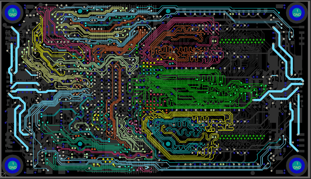
DC power supply PCB layout is an essential aspect of designing and building electronic circuits. The layout of a PCB can have a significant impact on the performance and reliability of a power supply. A well-designed layout can help reduce noise, improve efficiency, and minimize the risk of electrical interference.
When designing a DC power supply PCB layout, there are several key factors to consider. These include the placement of components, the routing of traces, and the use of ground planes. Proper placement of components can help minimize the length of traces and reduce the risk of interference. Careful routing of traces can help ensure that the power supply operates efficiently and reliably. The use of ground planes can help reduce noise and improve the overall performance of the power supply.
Basic Principles
When designing a DC power supply PCB layout, there are some basic principles that you should keep in mind. These principles will help you to create a reliable and efficient power supply.
Firstly, it is important to keep the input and output sections of the power supply separated. This means that you should place the input components on one side of the PCB and the output components on the other side. This will help to reduce noise and interference in the output signal.
Secondly, you should keep the high voltage components away from the low voltage components. This will help to reduce the risk of electrical shock and also reduce noise and interference.
Thirdly, you should use a ground plane on the PCB. This will help to reduce noise and interference in the output signal and also help to provide a stable reference voltage for the power supply.
Fourthly, you should use decoupling capacitors on the PCB. These capacitors will help to reduce noise and interference in the output signal and also help to provide a stable voltage to the components.
Finally, you should use high-quality components in your power supply design. This will help to ensure that your power supply is reliable and efficient.
Layout Guidelines
When designing a DC power supply PCB layout, there are certain guidelines that should be followed to ensure optimal performance and reliability. Here are some key considerations to keep in mind:
-
Minimize trace lengths: Keep trace lengths as short as possible to minimize resistance and inductance. This will help reduce voltage drops and noise.
-
Separate high and low current traces: Separate high and low current traces to prevent noise coupling and to reduce the risk of thermal issues.
-
Place decoupling capacitors close to the load: Place decoupling capacitors as close as possible to the load to reduce noise and improve transient response.
-
Use a ground plane: A ground plane can help reduce noise and improve EMI performance. Make sure to connect the ground plane to the chassis ground.
-
Use a star ground: Use a star ground to reduce noise and improve grounding. Connect all ground points to a single point.
-
Avoid sharp corners and right angles: Avoid sharp corners and right angles in traces to reduce the risk of EMI.
-
Use thick traces for high current: Use thick traces for high current to reduce resistance and minimize voltage drops.
By following these guidelines, you can design a DC power supply PCB layout that is optimized for performance and reliability.
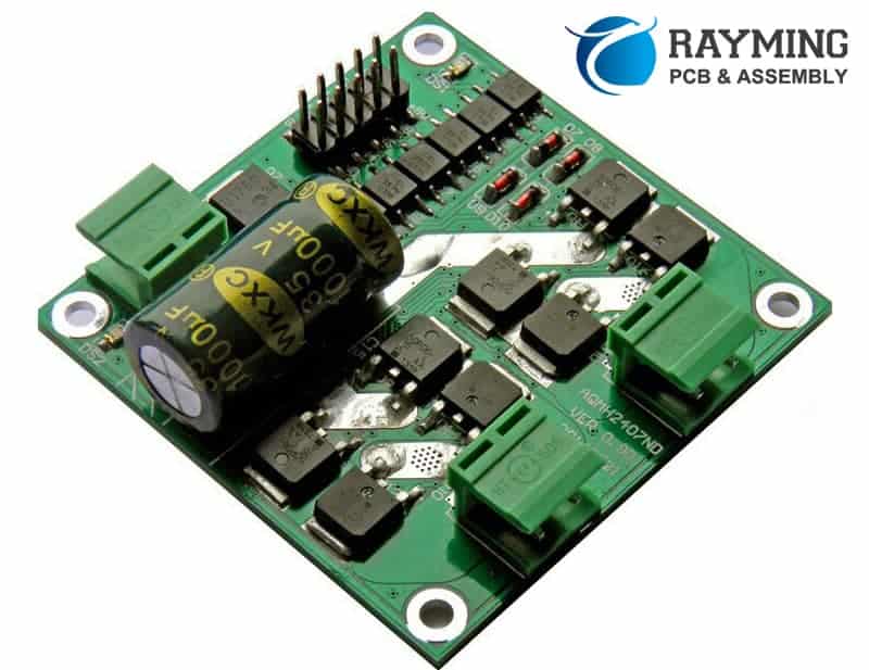
Component Placement

When it comes to designing a DC power supply PCB layout, the placement of components is crucial. Proper placement can help improve the performance and reliability of the power supply.
One important consideration is to place the power components, such as rectifiers, filter capacitors, and voltage regulators, as close to the transformer as possible. This reduces the length of the traces that carry high current and helps to minimize voltage drops and noise.
Another important factor is to group components according to their functions. For example, the input filter capacitors should be placed close to the rectifiers, while the output capacitors should be close to the voltage regulators. This helps to reduce the loop area and minimize the effects of parasitic inductance and capacitance.
It is also important to pay attention to the orientation of components, especially polarized capacitors and diodes. Make sure that the positive and negative terminals are correctly aligned and that the polarity markings are clearly visible.
In addition, it is a good practice to avoid placing components on the backside of the PCB, as this can cause interference and increase the risk of soldering defects. Instead, try to keep the components on the top side of the PCB and use vias to connect the traces on both sides.
Overall, proper component placement is essential for designing a high-performance and reliable DC power supply PCB layout. By following these guidelines, you can ensure that your design meets the required specifications and performs as expected.
Traces and Routing
The traces and routing are critical components of a DC power supply PCB layout. The layout should be designed to minimize the resistance of the traces and to reduce any inductance that may be present. This can be achieved by using wider traces and shorter routing paths.
When designing the traces, it is important to consider the current carrying capacity of the trace. The current carrying capacity is determined by the width of the trace and the thickness of the copper layer. A wider trace will have a higher current carrying capacity, and a thicker copper layer will also increase the current carrying capacity.
The routing of the traces should be designed to minimize the length of the trace. This can be achieved by placing the components as close together as possible and by using vias to connect the traces on different layers of the PCB. The use of vias can also help to reduce inductance in the traces.
It is also important to consider the placement of the components when designing the routing of the traces. The placement of the components can affect the performance of the power supply, and the routing of the traces should be designed to minimize any interference between the components.
In summary, the traces and routing are critical components of a DC power supply PCB layout. The traces should be designed to minimize resistance and inductance, and the routing should be designed to minimize the length of the trace and to minimize interference between components.
Grounding and Power Planes
The grounding and power planes are essential elements in DC power supply PCB layout. Proper grounding and power plane design can significantly improve the performance and reliability of the power supply.
Grounding
Grounding is critical for any electronic circuit. A good grounding scheme ensures that the circuit operates at the same reference potential, which minimizes noise and interference. In DC power supply PCB layout, the following guidelines should be followed:
- Ground should be a low-impedance path for the return currents.
- Ground traces should be as short as possible.
- Star grounding should be used to minimize ground loops.
- Sensitive analog components should be grounded separately from digital components.
Power Planes
Power planes are large areas of copper on the PCB that provide a low-impedance path for power distribution. Power planes can significantly reduce the inductance and resistance of the power supply, which improves the power supply’s stability and reduces noise.
In DC power supply PCB layout, the following guidelines should be followed when designing power planes:
- Power planes should be as large as possible to reduce resistance and inductance.
- Multiple power planes should be used to separate high-current and low-current circuits.
- Power planes should be connected to ground at multiple points to reduce noise.
By following these guidelines, the grounding and power plane design of a DC power supply PCB can be optimized for improved performance and reliability.
Signal Integrity Considerations
When designing a DC power supply PCB layout, it is essential to consider signal integrity. Signal integrity refers to the quality of the signal that travels through the PCB. Poor signal integrity can lead to noise, distortion, and other problems that can affect the performance of the circuit.
There are a few things to consider when designing a DC power supply PCB layout to ensure good signal integrity:
-
Keep signal traces short: The longer the trace, the more resistance, capacitance, and inductance it has. These parasitic elements can affect the signal quality. Keeping signal traces short can minimize these effects.
-
Minimize the number of vias: Vias can add parasitic capacitance and inductance to the signal path. Minimizing the number of vias can help maintain good signal integrity.
-
Separate analog and digital ground planes: Analog and digital circuits have different ground requirements. Separating the ground planes can help prevent noise from digital circuits from affecting the analog circuits.
-
Use decoupling capacitors: Decoupling capacitors can help filter high-frequency noise and provide a stable voltage source for the circuit.
-
Avoid sharp corners: Sharp corners can cause reflections and impedance mismatches, which can affect signal quality. Using rounded corners can help minimize these effects.
-
Place components carefully: The placement of components can affect signal integrity. Placing sensitive components away from noise sources and minimizing the distance between components can help maintain good signal integrity.
Overall, designing a DC power supply PCB layout with good signal integrity can help ensure the optimal performance of the circuit. By following these considerations, you can minimize noise, distortion, and other problems that can affect signal quality.
