GPS technology has revolutionized the way we navigate through the world. It has become an integral part of our daily lives, from helping us navigate to a new destination to tracking our fitness activities. GPS technology relies on a complex system of satellites, receivers, and software to provide accurate location data. One critical component of this system is the GPS printed circuit board (PCB) design.
The GPS PCB design plays a crucial role in ensuring the accuracy and reliability of GPS technology. It is responsible for providing a stable platform for the GPS receiver and other components to function optimally. The design of the PCB must take into account various factors such as signal integrity, noise reduction, and power management. A well-designed GPS PCB can help improve the sensitivity and accuracy of GPS receivers, resulting in better location data.
Basic Principles
GPS printed circuit board (PCB) design is a crucial aspect of creating a functional GPS device. A GPS PCB is a complex system that requires careful consideration of various design principles to ensure that it functions correctly. In this section, we will discuss the basic principles of GPS PCB design.
The first principle of GPS PCB design is to ensure that the GPS receiver has a clear view of the sky. This means that the PCB should be designed with minimal obstructions and should be placed in a location that provides an unobstructed view of the sky. Additionally, the GPS antenna should be placed in a location that provides a clear line of sight to the sky.
The second principle of GPS PCB design is to ensure that the PCB has a stable power supply. GPS receivers are sensitive to changes in voltage, and a stable power supply is essential to ensure that the device functions correctly. This can be achieved by using a voltage regulator or a battery backup system.
The third principle of GPS PCB design is to ensure that the PCB has a low noise floor. GPS signals are weak, and any noise on the PCB can interfere with the reception of these signals. This can be achieved by using high-quality components and minimizing the length of the signal traces on the PCB.
In summary, GPS PCB design requires careful consideration of various design principles to ensure that the device functions correctly. These principles include ensuring that the GPS receiver has a clear view of the sky, ensuring that the PCB has a stable power supply, and ensuring that the PCB has a low noise floor. By following these principles, designers can create GPS devices that are reliable and accurate.
Design Considerations

When designing a GPS PCB, there are several factors to consider to ensure optimal performance. Some of the most important design considerations are:
Antenna Placement
The placement of the GPS antenna is critical to achieving accurate location data. The antenna should be placed in a location that has a clear view of the sky to ensure it can receive signals from GPS satellites. Additionally, the antenna should be positioned away from any sources of electromagnetic interference (EMI), such as motors or power supplies, to prevent signal degradation.
Power Supply
The GPS receiver requires a stable and clean power supply to function correctly. It is essential to ensure that the power supply is free from any noise or voltage fluctuations that can affect the receiver’s performance. A voltage regulator can be used to provide a stable voltage to the GPS module and reduce the risk of voltage spikes or dips.
PCB Layout
The PCB layout plays a crucial role in the performance of the GPS receiver. The layout should be designed to minimize EMI and ensure that the GPS signal is not affected by other components on the board. The ground plane should be designed to provide a low-impedance path for any EMI and reduce the risk of interference.
Component Selection
The selection of components can also affect the performance of the GPS receiver. It is essential to choose components that have a low noise figure and a high gain to ensure that the GPS signal is amplified correctly. Additionally, the components should be chosen to minimize EMI and reduce the risk of interference.
In summary, designing a GPS PCB requires careful consideration of several factors, including antenna placement, power supply, PCB layout, and component selection. By taking these factors into account, designers can ensure that their GPS receiver provides accurate and reliable location data.
Components Selection
When designing a GPS PCB, selecting the right components is crucial for ensuring accurate and reliable performance. Here are some key considerations when selecting components:
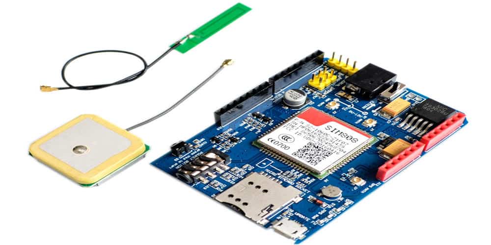
GPS Module
The GPS module is the heart of the GPS system and is responsible for receiving signals from satellites and calculating position information. It is important to choose a module that is compatible with your PCB design and meets your accuracy and sensitivity requirements. Some popular GPS modules include the u-blox NEO-M8N and the Skytraq Venus838LPx-T.
Antenna
The antenna is responsible for receiving GPS signals and is a critical component in determining the accuracy of your GPS system. Factors to consider when selecting an antenna include the frequency range, gain, and polarization. A popular antenna choice is the Taoglas MA245.A which has a gain of 25dB and a frequency range of 1575.42 MHz.
Power Supply
The GPS system requires a stable and reliable power supply to function properly. It is important to select a voltage regulator that can handle the power requirements of your GPS module and other components. The LM2937-3.3 is a popular choice for GPS PCB designs as it provides a stable 3.3V output with low dropout voltage.
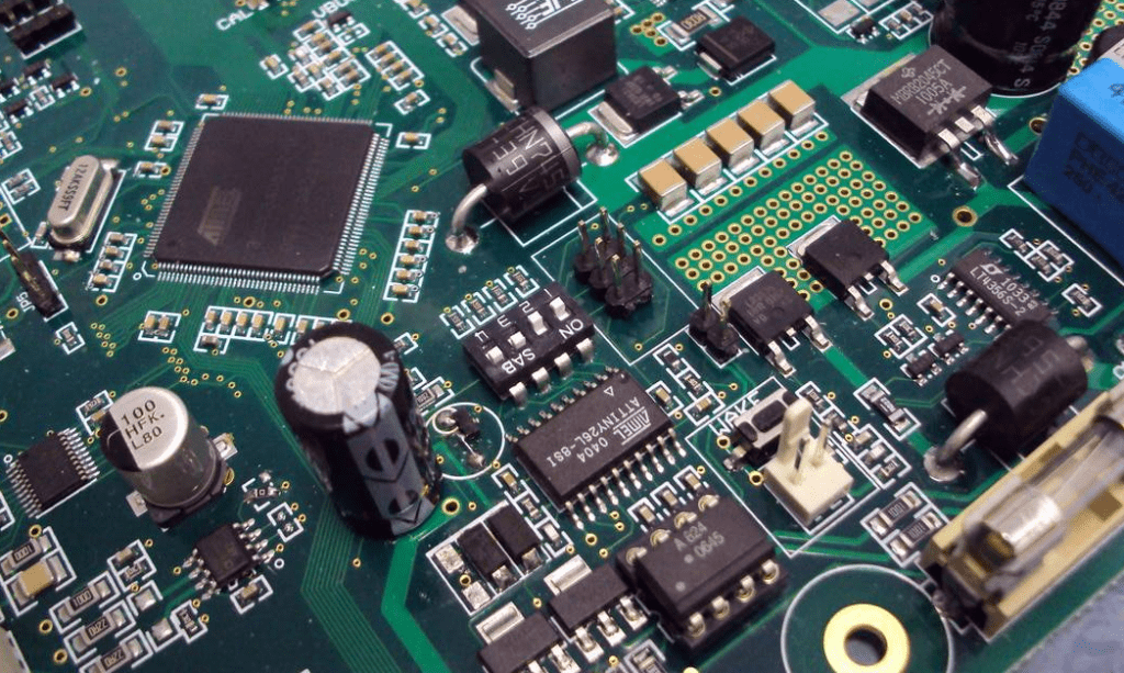
Passive Components
Passive components such as capacitors and resistors are essential for filtering and stabilizing the power supply and signal lines. It is important to choose components with appropriate values and tolerances to ensure stable and reliable operation. Some popular choices include the Murata GRM series capacitors and the Panasonic ERJ series resistors.
Overall, selecting the right components is crucial for designing a high-performance GPS PCB. By considering the factors outlined above and choosing components that are compatible with your design and meet your requirements, you can ensure accurate and reliable GPS performance.
PCB Layout
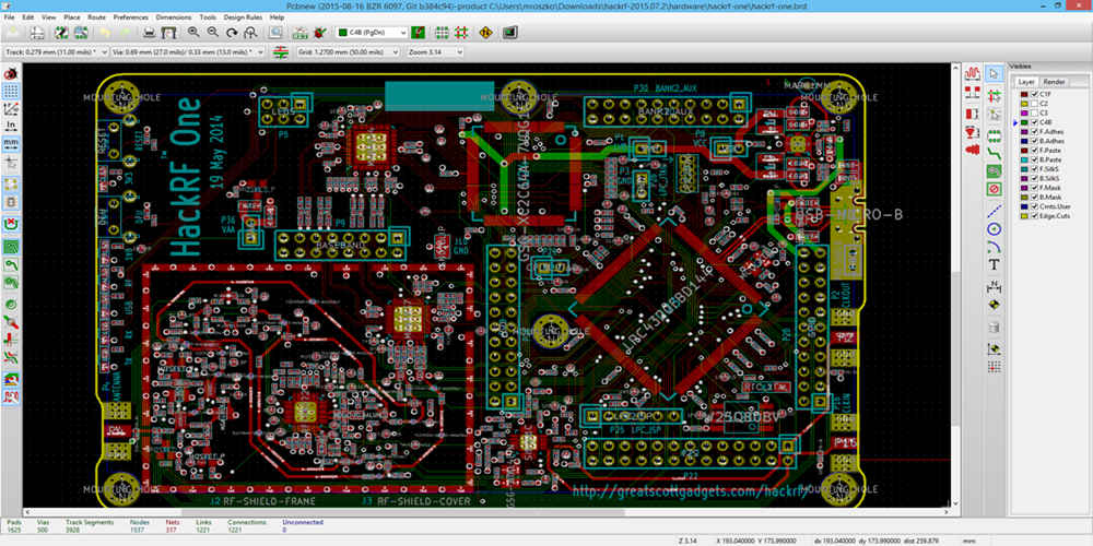
The layout of a GPS PCB is critical to ensure optimal performance. The main goal of the layout is to minimize noise and interference, which can affect the accuracy of the GPS receiver. Here are some important considerations for GPS PCB layout:
-
Ground plane: A solid ground plane is essential for reducing noise and interference. It provides a low-impedance path for return currents and shields the circuit from external noise. The ground plane should be placed on the bottom layer of the PCB and connected to the ground pins of all components.
-
Component placement: The placement of components on the PCB can affect the performance of the GPS receiver. The GPS antenna should be placed as far away as possible from noise sources such as switching power supplies and high-speed digital circuits. The GPS receiver chip should be placed close to the antenna to minimize signal loss and noise.
-
Trace routing: The routing of traces on the PCB is important for maintaining signal integrity. The traces should be kept as short as possible and routed away from noise sources. Differential traces should be used for the GPS signal to minimize common-mode noise.
-
Power supply: The power supply for the GPS receiver should be clean and stable. A low-dropout (LDO) regulator should be used to provide a stable voltage to the GPS receiver chip. Decoupling capacitors should be placed close to the power pins of the GPS receiver chip.
-
EMI/EMC: Electromagnetic interference (EMI) and electromagnetic compatibility (EMC) can affect the performance of the GPS receiver. Shielding can be used to reduce EMI and EMC. The PCB should be designed with proper spacing and grounding to minimize EMI and EMC.
In summary, the layout of a GPS PCB is critical for optimal performance. A solid ground plane, proper component placement, trace routing, power supply, and EMI/EMC considerations are important factors to consider when designing a GPS PCB.
Signal Integrity
Signal integrity is one of the most important aspects of GPS PCB design. It ensures that the signals transmitted and received by the GPS module are accurate and reliable. Any issues with signal integrity can lead to errors in GPS positioning, which can be disastrous in critical applications.
There are several factors that can affect signal integrity in GPS PCB design, including:
- Trace length: Longer traces can lead to signal degradation and increased noise.
- Impedance matching: Proper impedance matching between the GPS module and the PCB is crucial for signal integrity.
- Grounding: Proper grounding techniques can help reduce noise and improve signal quality.
- Power supply noise: Noise on the power supply can affect signal integrity and should be minimized.
To ensure good signal integrity, designers should follow best practices such as:
- Minimizing trace length: This can be achieved by placing the GPS module as close as possible to the antenna and using a four-layer PCB with a ground plane.
- Using proper impedance matching: This can be achieved by using a transmission line with a characteristic impedance that matches the GPS module and PCB.
- Using proper grounding techniques: This includes using a solid ground plane, minimizing ground loops, and separating analog and digital ground planes.
- Minimizing power supply noise: This can be achieved by using a low-noise voltage regulator and filtering the power supply with capacitors.
By following these best practices, designers can ensure that their GPS PCB designs have good signal integrity, resulting in accurate and reliable GPS positioning.
Testing and Validation
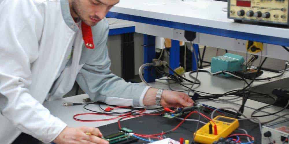
Testing and validation are critical steps in the GPS PCB design process. These steps ensure that the GPS system is functioning correctly and accurately. There are several methods to test and validate a GPS system, including simulation, field testing, and signal analysis.
Simulation testing involves using software to simulate real-world scenarios and test the GPS system’s performance under different conditions. This type of testing is cost-effective and allows for a wide range of scenarios to be tested quickly. Simulation testing can also identify potential issues and help optimize the GPS system’s performance.
Field testing involves physically testing the GPS system in real-world conditions. This type of testing is essential to validate the GPS system’s accuracy and performance in actual use cases. Field testing can also identify any issues that may not have been detected during simulation testing.
Signal analysis involves analyzing the GPS system’s signal to ensure that it is accurate and reliable. This type of testing can identify any interference or noise that may affect the GPS system’s performance.
To ensure accurate testing and validation, it is important to use high-quality testing equipment and tools. Additionally, it is essential to follow industry standards and guidelines for GPS testing and validation.
In conclusion, testing and validation are crucial steps in the GPS PCB design process. By using simulation testing, field testing, and signal analysis, designers can ensure that the GPS system is functioning correctly and accurately. High-quality testing equipment and adherence to industry standards are essential for accurate testing and validation.
