HDMI, or High-Definition Multimedia Interface, is a widely used technology for transmitting audio and video signals between devices. It is commonly found in devices such as TVs, monitors, and gaming consoles. The HDMI interface is designed to provide high-quality, uncompressed digital audio and video signals, making it an ideal choice for high-definition video applications.
One of the key factors that determine the performance of an HDMI interface is the PCB layout. The PCB layout plays a critical role in ensuring that the HDMI signal is transmitted with minimal loss and distortion. The PCB layout determines the placement of components and traces on the circuit board, which can affect the signal integrity of the HDMI interface. A well-designed PCB layout can help to minimize signal loss, reduce noise, and improve the overall performance of the HDMI interface.
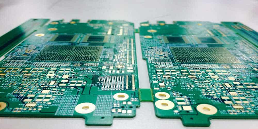
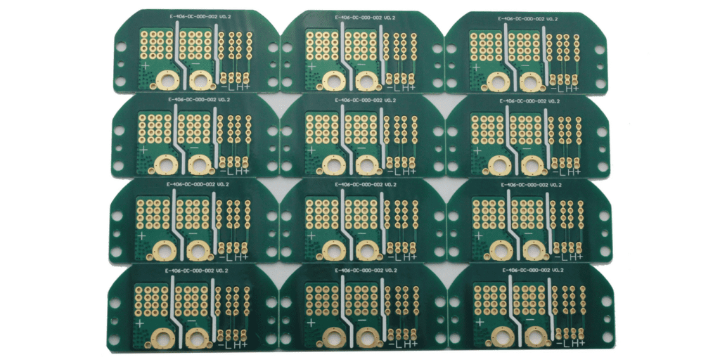
HDMI PCB Layout Basics
When designing a printed circuit board (PCB) for HDMI applications, it is important to consider the layout of the board. A well-designed layout can help ensure signal integrity and reduce electromagnetic interference (EMI).
Signal Integrity Considerations
Signal integrity is crucial for HDMI applications. To ensure signal integrity, it is important to minimize the length of the signal traces and keep them away from noisy components. The following are some tips for signal integrity considerations:
- Use controlled impedance traces to maintain signal integrity.
- Keep the differential pairs of HDMI signals as close together as possible.
- Avoid routing HDMI signals near noisy components such as switching power supplies.
Power and Ground Planes
Power and ground planes are critical for HDMI PCB layout. They provide a low-impedance path for current flow and help reduce EMI. The following are some tips for power and ground planes:
- Use a separate ground plane for HDMI signals.
- Connect the HDMI ground plane to the main ground plane at a single point.
- Place decoupling capacitors as close as possible to the HDMI connector to reduce noise.
In summary, designing a PCB layout for HDMI applications requires careful consideration of signal integrity and power and ground planes. By following the tips outlined above, designers can help ensure reliable HDMI performance.
HDMI Connector Placement

When designing an HDMI printed circuit board (PCB), proper connector placement is crucial to ensure optimal signal integrity and performance. The HDMI connector placement should be carefully considered before beginning the PCB layout process.
Physical Layout Guidelines
There are several physical layout guidelines that should be followed when placing the HDMI connector on the PCB. These guidelines include:
- The HDMI connector should be placed as close to the source device as possible to minimize signal loss and interference.
- The HDMI connector should be placed away from other high-speed signal traces to prevent crosstalk and electromagnetic interference (EMI).
- The HDMI connector should be placed on the edge of the PCB to allow for easy access and connection to the display device.
Connector Orientation
The orientation of the HDMI connector on the PCB is also important for optimal signal performance. The HDMI connector should be oriented in a way that minimizes signal reflections and maintains signal integrity. The following guidelines should be followed when orienting the HDMI connector:
- The HDMI connector should be oriented perpendicular to the PCB to minimize signal reflections and maintain signal integrity.
- The HDMI connector should be oriented so that the signal pins are facing away from the source device to prevent signal loss and interference.
By following these physical layout guidelines and connector orientation recommendations, designers can ensure that their HDMI PCB layout will provide optimal signal performance and reliability.
Trace Routing Guidelines
When designing an HDMI PCB layout, it is important to consider the trace routing guidelines. This section will cover the two main types of routing: differential pair routing and single-ended routing.
Differential Pair Routing
Differential pair routing is used for high-speed signals that require balanced transmission lines to minimize noise and crosstalk. Here are some guidelines for routing differential pairs:
- Keep the pairs as close together as possible to maintain balance and minimize impedance mismatch.
- Ensure that the pairs are routed parallel to each other with consistent spacing throughout the length of the trace.
- Avoid sharp turns, vias, and other discontinuities that can cause reflections and signal degradation.
- Use microstrip or stripline routing to maintain a consistent impedance throughout the length of the trace.
Single-Ended Routing
Single-ended routing is used for low-speed signals that do not require balanced transmission lines. Here are some guidelines for routing single-ended traces:
- Keep the traces as short as possible to minimize signal degradation and noise.
- Avoid running traces parallel to high-speed differential pairs to minimize crosstalk.
- Use ground planes or guard traces to shield the signal traces from noise and interference.
- Route power and ground traces separately from signal traces to minimize noise and interference.
By following these trace routing guidelines, you can ensure that your HDMI PCB layout meets the necessary signal integrity requirements for high-quality video and audio transmission.
EMI/EMC Considerations
When designing HDMI PCB layout, it is important to consider EMI/EMC (Electromagnetic Interference/Electromagnetic Compatibility) considerations to ensure that the device will function properly without causing interference with other devices.
Shielding Techniques
One of the most effective ways to reduce EMI/EMC issues is to use shielding techniques. Shielding can be achieved by covering the HDMI circuitry with a metal shield or by using a grounded enclosure. This will help to reduce the amount of radiated EMI that can escape from the circuit and interfere with other devices.
Filtering
Another effective way to reduce EMI/EMC issues is to use filtering techniques. This can be achieved by using EMI filters, which are designed to block unwanted frequencies from entering or leaving the circuit. These filters can be placed at the input and output of the HDMI circuitry to reduce the amount of EMI that can escape from the device.
Decoupling
Decoupling is another technique used to reduce EMI/EMC issues. This is achieved by using decoupling capacitors, which are designed to absorb high-frequency noise and prevent it from interfering with other devices. These capacitors can be placed at strategic points in the HDMI circuitry to help reduce EMI/EMC issues.
In summary, when designing HDMI PCB layout, it is important to consider EMI/EMC considerations to ensure that the device will function properly without causing interference with other devices. Shielding techniques, filtering, and decoupling are effective ways to reduce EMI/EMC issues and should be implemented in the design process.
Testing and Validation

Signal Integrity Testing
Signal integrity testing is a crucial step in the HDMI PCB layout process. It helps ensure that the signal quality is maintained throughout the transmission line. The testing process includes measuring the rise and fall times, overshoot, undershoot, and noise levels of the signals.
To perform signal integrity testing, you can use a high-speed oscilloscope, a signal generator, and a network analyzer. The oscilloscope helps measure the voltage and timing of the signals, while the signal generator generates test signals. The network analyzer measures the impedance of the transmission line.
EMI/EMC Testing
EMI/EMC testing is also an important step in the HDMI PCB layout process. It helps ensure that the PCB design meets the electromagnetic compatibility requirements. The testing process includes measuring the radiated and conducted emissions from the PCB.
To perform EMI/EMC testing, you can use an EMI receiver, a spectrum analyzer, and an anechoic chamber. The EMI receiver helps measure the radiated emissions from the PCB, while the spectrum analyzer helps measure the conducted emissions. The anechoic chamber helps reduce the external noise and interference during the testing process.
In summary, signal integrity testing and EMI/EMC testing are critical steps in the HDMI PCB layout process. These tests help ensure that the PCB design meets the signal quality and electromagnetic compatibility requirements.
