What does it mean when someone says he or she wants to make a design of a high frequency PCB? Most often, your thought process goes in the direction of making circuit boards that use higher frequencies than the traditional ones do. While that is the meaning, a lot of other concepts go into the making of a high frequency PCB design.
In this article, we do our best to break down this concept so you can have a better understanding that helps you make informed decisions when choosing this type of circuit board design.
What is a High Frequency PCB Design?
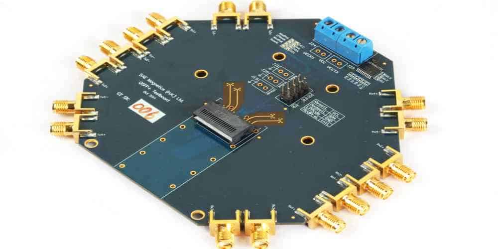
It is a type of Printed Circuit Board (PCB) that offers a faster signal rate than conventional PCBs do. Ideally, the signal flow rate is based on the electromagnetic frequency, ranging between 1 and 10 GHz.
The flow of signals is one essential factor in the consideration of a circuit board design. Due to the routing/traces and the number of components added to one box, it is expedient to have the signals passing on from one part to the other.
The speed at which this is done determines how efficient the circuit board would function. Thus, using a high frequency PCB design goes a long way to bolster signal transmission, keep the components’ functions in top gear and facilitate real-time operations of the electronic devices.
Laminate Material Considerations
Due to the defined and more advanced capabilities, it is expected that the laminate materials used for this type of PCB are different from what we are used to.
It is common to use materials that offer a mix of low loss tangent, low constant dielectric properties, advanced composites, lower attenuation and high CTE. It is also important to choose the laminate materials that offer the following:
- Water absorption capabilities
- High efficiency and;
- Low dissipation factor
It is also important to note that despite the higher efficiencies, water absorption and low dissipation capabilities, the materials used for the high frequency may also differ. The differences often stem from the environment/application of the circuit board and the required signal speeds.
Therefore, going for the right selection of materials for the targeted applications is a must. The following are examples of the popular materials you can use for the design:
- Teflon and Flex substrate materials: these are the best for the high frequency PCB designs that require above 10 GHz of frequency. Some of the attributes of these materials are survivability in the immediate environment/application, Dk, water absorption and Df. These new-generation substrates also tend to offer advanced functionalities than the traditional FR-4 materials do.
- Panasonic Megtron6: this is a PCB material from Panasonic Industry. It is used because of the low loss transmission and the suitability for the over 3 GHz of operating frequency.
- FR-4 materials: the popular Flame Retardant 4 (FR4) materials are also a top choice for the high frequency PCB design. The major advantages are the capability to manage heat and affordability. However, in terms of the usage for higher frequencies, you cannot entirely rely on the materials, as they hardly bolster signal speeds above 1.6 GHz.
- Tachyon, Isola I-Speed & Isola Astra: these 3 laminate materials are the ideal choice for high frequency PCB designs that require low loss even when operating at higher frequencies.
- Rogers 4350B: this high frequency PCB material can facilitate signal rate transfer for applications requiring a frequency between 500 MHz and 3 GHz.
Note that not all PCB material manufacturers offer the laminates that can be used for high frequency design. If you are looking to buy these kinds of materials, your best option is to purchase from the following manufacturers:
- Panasonic Industry
- DuPont
- Isola
- Rogers
- Taconic and;
- Tachyon
High Frequency PCB Design Rules to Have in Mind

If you must achieve a considerable success with this design, you must follow some of the design iterations. These rules should put you on the spot and help you make the most out of your high frequency PCBs:
1. Avoid Trace Bends
Being the traces or putting them in a non-straight-line position is not the best option. Sticking to this pattern only aids in the reduction of impedance.
A better way to go about it is by keeping the PCB wires straightened. This does not only help in the continuity of the impedance, but also bolsters the coupling of the high frequency signals.
It is also possible to opt for a 45-degree bend, which is the process of straightening the PCB wires with 45-degree corners. This also changes the circuit’s shape to an arc shape.
By going for the arc shaped design, you now position the PCB to reduces the chances of having external emissions. At the same time, it helps to enable the mutual coupling of the high frequency signals.
2. Make a Signal Ground Isolation
It is pertinent to isolate the digital signal ground from the analog signal ground. This is because the two have a number of substantial differences in the voltages.
Another good reason to make the separation is because of the tendency of the higher digital signals that would likely affect the analog signals at the PCB’s ground plane.
3. Separate the Signals’ Power Supply
Just as we separated the digital signal ground from the analog signal ground, we should also do the same for the power supply.
This separation is encouraged by the fact that the power supply, which is designed in layers, could shield crosstalk.
Therefore, the separation should be done thus:
- A separate power supply should be set up for the analog signals and the digital signals.
- This power supply separation should only be done if the PCB has both the digital and analog signals.
4. Reduce the Usage of Vias
The number of vias used for the high frequency PCB design should be kept at the barest minimum. This is because having a mixture of multiple vias and straight corners tends to trigger discontinuation of impedances to the PCB wires.
Considering the vias’ 0.5 pF distributed capacitance, the reduction or non-usage goes a long way to cut down on the possibilities of encountering data error, while helping the speed of signal transmission.
However, if some reason, you must use vias in the PCB design, make sure it is distanced from the signal lines or PCB wires. That way, there wouldn’t be much impedance discontinuities that aggravate signal integrity issues in the board.
5. Loop Usage Should be Discouraged
It is better not to use loops in the high frequency PCB design. The reason is because of the loops’ design that encourages the enclosure of the signal path.
Considering that the goal of a high frequency PCB design is to facilitate signal transmission rates, it doesn’t make sense to use a device that reduces the chances of that from happening. Therefore, loops should be removed from the high frequency PCB design to prevent crosstalk.
Just like the vias, if the loops must be used, they need to be limited to a smaller area to enable the flow of signals in the circuit board.
6. Impedance Matching Should be Accurate
Getting the right impedance is one way to bolster signal flow in a high frequency PCB. The best way to match the impedances is by keeping them operating at the same pace. This way, the board would be free of the following challenges:
- Undershooting
- Ringing and;
- Overshooting
7. Reduce the Use of the FR-4 Materials
Although the Flame Retardant 4 (FR-4) materials can save costs and improve signal transmission, if you can avoid using them, do so.
It is because of the following reasons:
- The material has a steeper Dk versus frequency response curve, when operating at the higher frequencies.
- FR-4 materials tend to exhibit higher dielectric losses.
8. Use Paralleled Wires with Enough Spaces
It is almost impossible to avoid the use of paralleled wires in circuit boards and this could lead to crosstalk.
Nevertheless, you can optimize the wires for the best performances. One way to do that is by use shorter paralleled wires. Not only that – there should be sufficient space between them.
Implementing this design helps to cut down on the “mutual effect” between the electromagnetic fields of these wires.
9. Avoid Crosstalk in High Frequency PCBs
We have mentioned crosstalk severally in this article. What does it mean? Crosstalk, in PCB, refers to the unwanted noise signals that emanate between the signal lines. It emanates primarily because of the coupling of the electromagnetic fields in these signals.
Therefore, reducing the crosstalk has a lot to do with the layout process of the circuit board. Before talking about the reduction options, note that some of the common influences are:
- The spacing of the signal lines
- PCB plate layer’s parameters
- The signal line connection mode and;
- The electrical characteristics of the load and source terminals.
Haven noted the common factors triggering crosstalk in high frequency PCB design, here are some of the options to reduce it:
- A center-to-center separation between the two traces should be maintained. This should be done in a way that the separation should be at least three times the traces’ width.
- A perpendicular routing of the clock line should be done rather than the parallel format.
- There should be a considerable distance between the low voltage differential clock signal and the high frequency signal clock.
- A ground plane or ground line can be inserted between the two signal lines that have a serious crosstalk.
The Challenges to Making High Frequency PCB Design
No doubt that the design for a higher frequency can improve the speed of signal transmission in a circuit board. However, certain concerns might arise in the cause of doing so.
Here are some of the common challenges peculiar to high frequency PCB design:
Coupling
This happens when two conductors or signal lines are approximate or close together. The best way to prevent coupling in your high frequency PCB is by spacing the conductors.
Radiation
Due to the composition of components or laminate materials that have EMI capabilities, it is possible for the high frequency circuit board to be prone to radiation.
A better way to manage this is to use the devices (such as power suppliers and wireless transmitters) in the environments where they are not always prone to EMC and EMI.
Excessive Reflections
Reflections becomes excessive or higher in a high frequency PCB design when the impedances do not match.
When the impedances are accurately matched, it reduces the chances of having the originating signals being sent back to the source.
Common Mode Noise
This is common when there are more stray capacitances between the terminals. The issue of Common Mode Noise is common with the Printed Circuit Boards (PCBs) that have either of the following:
- Conversion circuitry
- Power supplies
The Benefits of Taking to High Frequency PCB Design
Despite the challenges and some of the dexterous design iterations, making high frequency circuit boards is worth it.
Here are some of the advantages of this type of PCB design:
- Excellent Tolerance Rate: this is the best type of PCB design to use for applications exposed to harsh weather conditions. The excellent tolerance rates of the high frequency PCB design include an outstanding peeling strength, moisture resistance and chemical corrosion resistance.
- Increased Efficiency: the primary efficiency of the board is the improved signal transmission rate. The others are improved environmental protection and the capability to meet most of the heating requirements of most applications/devices.
- Temperature Control: since most of the applications and use cases are for industrial devices, using a high frequency PCB design helps to manage the higher temperature requirements of those devices.
- Improved Transmission Speed: this is the major reason why you want to get a high frequency PCB. The speed of transmitting or moving the signals is a major plus.
Wrapping Up
High frequency circuit boards speed up the processes of signal transmission, tackle some of the issues relating to signal integrity and regulate the temperatures of devices exposed to metal heating.
Hillman Curtis makes the best high frequency PCBs, taking into account, the preferred use cases, your budget and the additional customizations you want on the board.
