Printed circuit boards are the backbone of most electronic devices. Without them, electronic devices won’t function. A high frequency PCB is one of the most frequently used PCBs in the electronic industry. High frequency PCBs have got some unique properties that make them ideal for use in several applications.
This article aims to discuss important facts about high frequency PCBs. The demand for faster signal flow rates is increasing in the electronic industry. Therefore, the need for high frequency PCBs have continued to increase.
What is High Frequency PCB?
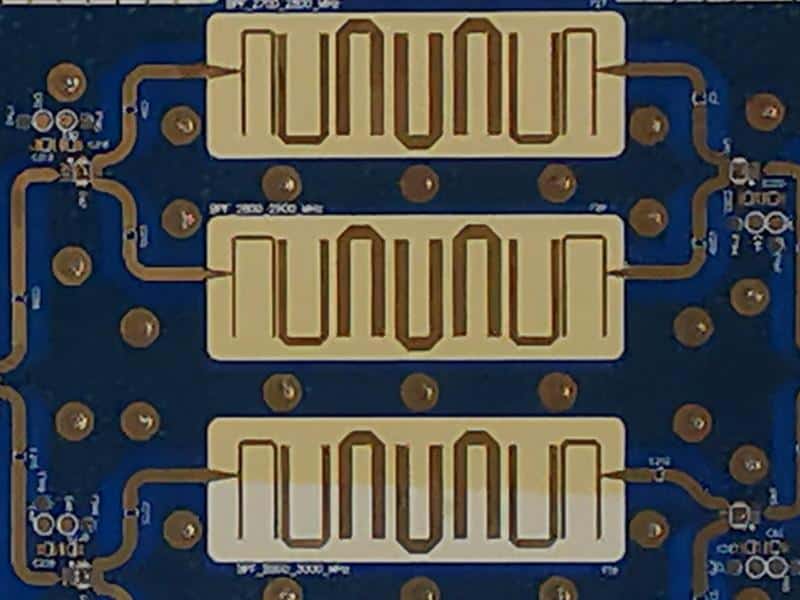
A high frequency PCB is ideal for use in applications that demand high signal transmission between objects. This type of circuit board has a frequency range of 500 MHZ to 2 GHZ. Due to its properties, it is common in high speed applications. The production of high frequency boards requires special materials since manufacturers need to attain high frequency.
Today’s electronic components require faster rates of signal flow. High frequency PCBs can transmit signals at longer distances. Therefore, it is ideal for use in radar systems and communication industries. Any application that requires signal transmission between two objects is high frequency boards.
Request High Frequency PCB Quote, Pls send PCB files to Sales@raypcb.com Now
Properties of High Frequency PCB
To have a vivid understanding of high frequency boards, you need to know its properties. This helps you to know what high frequency PCBs are capable of. Below are some of the properties of high frequency boards.
Dielectric constant
High frequency PCBs feature low and stable dielectric constant. This property helps to prevent any delay in frequency signal transmission. Dielectric constant is the ability of a laminate to save electrical energy. This measure changes in line with the axis of the material.
Low dissipation factor
This is another property of high frequency PCB. The dissipation factor of a high frequency board influences the quality of signal transmission. To achieve clearer and faster signal transmission, a low dissipation factor is advised.
Excellent Coefficient of thermal expansion
The CTE of a material refers to how temperature affects its size. Some materials will expand when exposed to some temperatures. CTE is the best way to detect the thermal robustness of a laminate. This measure plays a significant role during the manufacturing process of high frequency PCBs.
High-frequency PCBs feature excellent CTE. Due to this property, these circuit boards are ideal for use in applications subjected to varying temperatures.
High chemical resistance
When it comes to the ability to resist chemicals, high frequency PCBs have it. These circuit boards can withstand chemical attack. They are corrosion-resistant. This makes them a perfect choice in some applications.
Loss tangent
Loss tangent is an important property of a high frequency PCB. The change in the molecular structure of a laminate refers to the loss tangent.
High Frequency PCB Design Guidelines
High frequency PCB design requires manufacturers to put certain things in check. This process requires a lot of planning. Therefore, it is important to follow some guidelines for your high frequency PCB design.
Plan the design
This is the first step in creating a high frequency PCB design. Prior proper planning helps you create a good design. Planning a design prevents any setbacks during the design process. You can get a checklist for the design.
Determine the board’s signal frequency
This step is crucial in creating a high frequency PCB design. Document the voltage and power requirements for the integrated circuits. Determine if there is any need to divide any power planes. Check if your design can accommodate various signals and trace length. The manufacturer needs to reveal what their requirements for minimum tolerance are.
Document Stack Up plan for your board
You need to put down the stack up layer’s requirements. Your manufacturer will have to help you determine the requirements for your boards. Understanding the PCB materials and the constraints of the circuit board is important. You can create other plans for your stack up.
Floor planning
You will need to divide your circuit board into logical parts. You have to consider if you will be placing all circuits into a bigger design. This is very important, especially when there are digital and analog areas you need to isolate. Isolation will help to reduce interference in this case.
Know your power and ground planes
You need to understand the power and ground planes of your design. The manufacturer will have to create partitions on the ground plane. This involves rotating the void that might have an influence on the signal timings and EMI. Make sure you add a resistor alongside the signal trace.
Route the high-frequency signals
To get more shielding benefits, it is advisable you route your frequency signals. As you move the high frequency signals from the source, they will release high amounts of radiation. This situation can cause interference between two signals. You can prevent this from happening by routing the frequency signals.
Create enough current return path
High frequency PCBs have signals that need a route. Ensure the path remains smooth. To achieve this, you will need vias. The current may likely spread over the splits if you don’t do this.
These high frequency PCB design guidelines will help you go through the design process smoothly. It is important you carry out each step carefully to achieve a great design.
Request High Frequency PCB Quote, Pls send PCB files to Sales@raypcb.com Now
Where is High Frequency PCB Used?
High frequency PCBs are suitable for use in applications that require high performance. These PCBs can survive high heat and temperature. Most electronic devices today feature high frequency circuit boards. These boards are used in the following industries;
Medical industry
Most medical devices feature high frequency boards. These boards have contributed to the development of electronics in the medical world. Some diagnostic, treatment, and monitor devices feature high frequency boards. This circuit board is known for its ability to transmit signals quickly and as such, it is used in the production of some medical devices. For example, ultrasound scanners, X-ray machines, and microscopes feature this type of PCB.
Advanced communication system
Since high frequency PCBs can have faster signal transmission rate, they are used in this application. These boards allow clear transmission and as such are effective for communication devices. Devices like mixing decks, booster stations, and microphones feature this PCB type.
Military industry
High frequency PCBs are found in most military devices. Ammunitions and firearms feature this type of PCB. Manufacturers of military devices use this PCB due to its ability to tolerate high temperature.
Industrial applications
The use of high frequency PCB is common in this application. These circuit boards have great mechanical and electrical properties. They can withstand different chemicals and high heat. Most industrial devices are subjected to harsh temperatures, hence the use of PCBs for their manufacturing. Measuring equipment, electric drill, and power indicators feature high-frequency boards.
Radar systems
High-frequency PCBs are widely used in radar systems. These PCBs have come a long way in the marine and aviation industry. The radar systems are used in sailing and underwater applications. These systems help ships to prevent obstacles like icebergs. Sailing vessels also feature this type of PCB. The radar system guides aircraft and as such, helps to prevent accidents.
High Frequency PCB Material
For the production of high frequency boards, several materials are required. Since these boards transmit high signals, they feature special material for their production. The materials below can be used for your high frequency boards.
Rogers
Rogers materials are very rich in quality. This PCB Company has got branches across countries in Asia and Europe. Rogers introduced the RT/duroid material which is now the best option for high frequency PCB material. This company delivers laminates that can be used to fabricate high frequency PCBs.
FR4 is a common high frequency PCB material you can buy from this company. This material features glass fiber foil at both sides. FR4 material is ideal for use in applications that demand high-frequency features. Although Rogers materials are quite expensive, the quality is top-notch.
Isola
Isola is a well-known brand in the PCB industry. This company designs copper-clad laminates. These laminates are ideal in the fabrication of high-frequency PCBs. Isola has companies in the US, Europe, and Asia. The high frequency boards produced by Isola have proved to be of good quality.
Arlon
Arlon is one of the best producers of high-frequency laminates. These laminates feature unique electrical and mechanical properties. Arlon majorly deals in thermoset resin technology. Its PCB materials have been used in microwave PCBs, military electronics, and other high frequency applications. This company is ISO 9001: 2008 certified. It works in line with the standards of the PCB industry.
Hitachi
This is another manufacturer of high frequency PCB materials. Hitachi is a reliable PCB company that delivers a wide range of PCB materials. These materials are ideal for high frequency boards. They have been tested and they have proved to be of good quality.
GIL Taconic
This company is one of the leading producers of high frequency PCB materials. GIL Taconic has several manufacturing plants in countries like France, Korea, Brazil, and the US. These materials feature a high temperature and chemical resistance. They are also known to have properties like minimal electric losses and high dielectric strength.
Selecting the Best Material for High Frequency Boards
The fabrication of high frequency PCB is a very complex one. Therefore, it is very important you choose the best circuit material. Several factors determine the choice of material to use. However, there are two major factors that determine the type of material to use. Firstly, the effort required to fabricate a circuit using a particular material. Secondly, how these materials meet the demands of an end-use application.
Furthermore, there are some factors you need to consider when choosing materials for high frequency PCBs.
Type of material
There are several manufacturers of high frequency boards. But, not all of them offer quality. It is important you consider the manufacturer of the material you are opting for. Ensure you get your materials from the best brands. Rogers, Isola, and Arlon are examples of the manufacturers you can choose.
Spacing
Proper spacing plays a great role in your high frequency board. This is particularly important when it comes to the skin effect and cross-talking of a board. Crosstalk happens when the circuit board begins to self-interact. Skin effect directly correlates with trace resistance. The skin effect increases when there is an increase in trace resistance. When this happens, the PCB begins to warm up.
Coefficient of thermal expansion
This is an important factor to evaluate when choosing the best materials. CTE measures how a material responds to temperature. It measures the size of a material in response to temperature. Ensure your substrate has the same CTEs. When you have different CTEs, the components of your board may expand.
Dielectric constant
The dielectric constant is a measure of a material’s ability to save energy in an electric field. The dielectric constant plays a significant role in selecting the best material for high frequency PCBs.
Request High Frequency PCB Quote, Pls send PCB files to Sales@raypcb.com Now
High Frequency PCB Manufacturing Process
The manufacturing of high frequency PCB is a complex one as special materials are used. Achieving the best quality requires taking some fabrication instructions. When fabricating this type of PCB, special processes are required. These steps will help you go through the manufacturing process.
Design the board
This is the first thing you need to do. Here, you must have a sketch of where you intend to lay the blueprint of your circuit board. There are softwares that helps you create nice designs. For example, the Extended Gerber can help you encode the necessary details you need. Confirm some areas of the design after encoding the blueprint.
Print the design
After designing the board, the next step is to print the design. A plotter printer prints the design for you. This printer releases the film of the board which is the negative of the circuit board.
Copper printing
This is where you start the manufacturing process. Here, the copper will be pre-bonded on the same laminate. You will use the laminate that serves as the board’s structure. Then you reveal the initial blueprint of the circuit board. After, you use a resist to conceal the laminate panel. The resist contains a photoreactive chemical layer.
You will need to line up the resist and the laminate and subject them to ultraviolet light. When the resist hardens, you will be able to locate the copper areas.
Layers alignment
In this stage, you have to align the layers. The holes can help you align the outer and inner layers of the board. An optical punch machine can help you achieve this. The manufacturer puts the layers on top of the optical punch. This machine aligns the board’s layers by inserting a pin through the holes. After this process, you can check for any defect in your PCB by using the AOI machine.
Lamination
In this stage, you will fuse the layers of the board. The outer area of the board consists of fiberglass. The original material of the circuit board is covered by a copper foil. Use a metal clamp to fuse the layers together. Place a pre-coated epoxy resin layer and then a layer of substrate and a copper foil layer. The lamination process begins after joining the layers. The manufacturer uses a heated plate to transmit pressure and heat to the layers. The pressure joins the layers while the heat melts the epoxy.
Drilling
The manufacturer needs to locate the spots to drill. You can make use of an X-ray machine to locate these spots. You have to drill guiding holes. These holes secure your boards. A computer-guided drill will help you drill the holes perfectly.
Plating
This process involves using chemicals to fuse different layers. The circuit boards need to be cleaned before putting them in several chemicals. This will enable you to coat the panel and cover the walls of the drilled walls.
Outer layer plating
Here, you will need to apply the resist to the outer layer. It is important you plate the inner layer of the PCB. Outer layer plating helps to shield the copper on the outer side.
Solder Masking
Clean the panel before applying a solder mask. Add an epoxy ink with the solder film. Expose the circuit board to ultraviolet light.
Silkscreening
This process involves printing important details on the board. You will have to print the warning labels, the company ID number, and the manufacturer’s marks.
Testing
After you have done everything, you need to test the board. This stage is very important as it helps to confirm the efficiency of the board. PCB manufacturers employ different testing methods. You can employ electrical testing, visual testing, or use X-ray. Some manufacturers employ all testing methods.
