High speed PCB design refers to any design where the physical properties of your PCB, such as its layout, packaging, connectivity, layer stackup, and other features, start to affect the integrity of your signals.
As you start designing the boards and run into issues like delays, crosstalk, reflections, or emissions, you’ll also enter the world of high speed PCB design.
Because of the focus on these difficulties, high speed design is so special. You may be accustomed to designing a straightforward PCB where the major focus is on component routing and placement.
However, it’s more crucial to consider a few things when utilizing high speed design, such as how close they are to signals, what width they will be, where you are placing the traces, and what kinds of components they are connected to. Additionally, when you take these aspects into mind, your PCB design process will succeed at a high level.
Today, it can be said that the majority of PCBs are susceptible to various signal integrity issues, which are typically connected to high speed digital design. The goal of high speed PCB design and high speed layout is to provide circuit board designs that are less prone to issues with signal integrity, power integrity, and EMI/EMC.
However, what do signals mean exactly, or what does signal integrity mean? It will be important to understand this in the further exploration of what high speed PCB design is all about.
Because they can operate with integrated circuits at high speeds for the majority of devices in the electronics industry, even fairly simple ones, high speed PCB design is in high demand as electronic technology advances.
There are certain variables and aspects that are taken into account when designing a high speed PCB. Any design you are working on will transmit some sort of signal along the lengths of your copper traces to a specific location. There are analog and digital signals and the signal can be one of the two.
Types of High Speed Signals
Digital signals
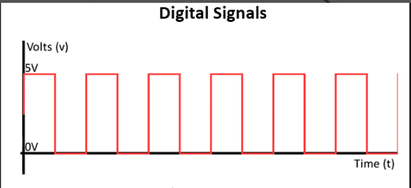
Every digital system known to man uses what is known as a digital signal, sometimes known as a square wave or clock signal.
A digital signal gives a considerably simpler representation of values by just having a high point and a low point, or 1 and 0, or being on or off, as opposed to analog signals, which can have values scattered all over the place.
The waveform of a digital signal would appear so simply on a graph where the high point and low point will be easily noticeable to denote the on and off points of a circuit.
Analog Signals
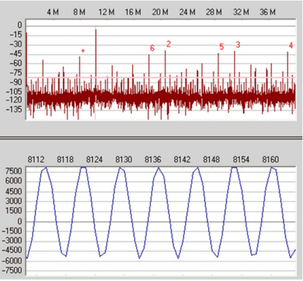
Signals classified as analog have a specific range of positive and negative values. Analog signals can produce a range of outcomes depending on their signal intensity and frequency, unlike digital signals, which are simply a set of on and off points.
The waveform of an analog signal can vary greatly depending on its amplitude and frequency as seen on a graph. Signal Integrity (SI), which bothers on interference in digital and analog signals, is important. Problems occur when an environment influences a signal.
Take a net for instance, that transfers data containing signal from point A to point B on your PCB layout. Point A is the signal’s transmitter, while point B is its receiver, according to this definition. The integrity of your signal may be compromised by a variety of factors between points A and B, including:
Signal Reflection
This occurs when a signal is being transmitted over a copper trace and a portion of the signal is reflected back to its origin instead of continuing on to its final destination.
Signal Ringing
This occurs when there is an unintentional change in the voltage or current on your trace, which results in an increase in current flow and delays the arrival of your signal at its intended location.
Signal Noise
This occurs when a signal on your board has an arbitrary fluctuation that may have an impact on nearby signals. The data in a signal can be affected when there is a lot of noise impacting it.
Signal Crosstalk
This occurs when two copper wires or traces are placed too closely together, causing electromagnetic radiation from one transmission to interfere with the other signal and corrupt the data.
Signal Timing
This occurs when high speed signals are sent, but they do not arrive at their destination in time to match up with the clock signal. If this occurs, your signal can be read as a 1 even though it was intended to be a 0.
These are but a few of the many common issues that may arise and tamper with signal integrity across a distance in the circuit. Of all of them, the three top concerns are:
- Timing: Are all the signals on your PCB layout reaching at the appropriate times in respect to other signals, in other words? A clock controls each high-speed signal on your board layout, so if your timing is incorrect, you can be getting distorted data.
- Integrity: When your signals reach their final location, do they appear as they should? If they don’t, your signal most likely ran into interference along its path that compromised its integrity.
- Noise: Did interference of any kind affect your signals as they traveled from transmitter to receiver? Every PCB produces some level of noise, but when this noise is excessive, the⁴ 4th of data corruption increases.
In the case that any if these three show up in the transmission of a signal, there are three big ways to deal with each of them.
- Impedance: The integrity and quality of your signals will be directly impacted by the correct impedance between your transmitter and receiver. Your signals’ noise sensitivity will be impacted by this as well.
- Matching: Your traces will arrive at the same time and in sync with your clock rates if the lengths of two connected traces match. For applications including DDR, SATA, PCI Express, HDMI, and USB, matching is a crucial option to consider.
- Spacing: Your traces are more vulnerable to noise and other types of signal interference the closer they are to one another. You can lower the noise on your board by not positioning your traces any closer together than necessary.
How to Know if Your PCB Project is High Speed

The criteria for a PCB to be considered high speed are not well defined. In the end, each situation must be evaluated on its own merits. You can tell you’re working on a high speed project if you’re having some signal integrity problems with your PCB layout.
You will undoubtedly be working on a high speed project if you are building a motherboard, a cell phone board, or a DSL router board.
Additionally, be aware that you will face high speed design restrictions if you need to integrate any of the following technologies into your layout: HDMI, PCI Express, USB, or SATA.
The final factor to take into account is whether the design you are working on uses lumped or distributed circuits. Lumped system typically doesn’t come with PCB design complexities, but in a distributed system, designers will have to concern themselves with high speed PCB designs.
There’s some knowledge that designers need to have in their arsenal in the creation of high speed PCB and it’s high speed components.
High Speed PCB Designer Skills
- Knowledge of high speed PCB design software that offers advanced options: Your CAD program needs a lot of intricate functionality for high speed designs. There may not be many pursuit-oriented programs, particularly ones with sophisticated features built on Web suites. Consequently, you must gain a deeper understanding of a powerful CAD tool.
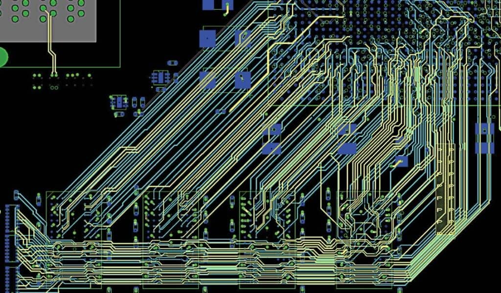
- High Speed Routing: A designer needs to be aware of the basic routing guidelines for high speed traces, such as not cutting ground planes and keeping trails short. In other words , keep digital lines a specified distance apart to avoid crosstalk, and protect the signal integrity from any devices that can cause interference.
- Impedance control when routing traces: For some signal types that range from 40 to 120 ohms, impedance matching is required. The existence of antennae and the availability of several differential pairs are distinguishing characteristics of impedance match.
For the requisite impedance values, a designer must understand how to determine trace width and layer stack. If the impedance value is incorrect, the signal may be severely hampered, which will cause data corruption. - Eliminating loop areas: High frequency signals will cause some EMI/EMC issues. High speed PCB designers must be aware of this fact. Knowing this, they must follow fundamental high speed design guidelines like having continuous ground planes, decreasing loop sizes, and optimizing current return paths for traces in addition to including lots of stitching vias.
Some Factors to Consider Before Embarking on High Speed PCB Design
- Considerations for schematics: As you are aware, a strong schematic can serve as a solid base for PCB design. D epending on whether you are an electrical engineer or a PCB designer, you can approach the schematic in a different way.
Generally, the schematics are viewed as a channel of communication with the board, but it How can significantly impact how you organize and display your high-speed design. Therefore, considerations on the trace lengths, component locations that are necessary, PCB manufacturer information, and so forth, have to be brought into account. - Trace length tuning: When using a high speed interface, you must tune the length of the traces to align signal transmission with data lines. When out of sync, the interface may malfunction at the highest frequency or cease to function altogether.
Additionally, the need for length matching increases with the frequency of the interface. Therefore, in the case of a parallel interface, you only need to adjust the lengths of all the traces. In order to obtain the appropriate lengths within a collection of signals, it is crucial to consider tuning those trace lengths. - PCB materials and stackup requirements for high speed: These factors, such as the structure of the layer stackup and the materials used to construct your PCB, will have an impact on your high speed design.
- High speed placement techniques: Because changing pad dimensions and component clearances can have an impact on reducing high speed connection lengths, it is possible to optimize component placement with a variety of high speed design techniques. It is also possible to improve component footprint enhancements to achieve high speed.
- Differential pair and trace length routing: It’s crucial to have differential pair routing in a high-speed architecture so that paired signals can travel at the same time. This is known as trace length routing.
Crosstalk, impedance management, and parallelism considerations are just a few of the numerous factors that might negatively impact a high-speed design. Additionally, some questions must be taken into account, such as how to reduce the impact on your design. - Understanding stripline vs. microstrip: Generally, high speed systems require a different approach to trace routing. You’ll need to have a deeper understanding of stripline and microstrip routing strategies if you wish to accomplish high speed routing.
- Routing topologies and best routing practices: in general, specific forms or topologies must be used if you wish to accomplish the required circuit path for high speed routing. Additionally, it is fantastic to investigate different approaches to routing with trace lengths, escapes, return pathways, and other variables.
- Simulators: For high speed designs, simulation is very useful prior to, during, and after the layout. In order to discover the tips and tricks used to simulate your designs, you should have a better understanding of your PCB design program.
In order to maintain signal and power integrity, PCB stackup design and routing take center stage in high speed design. The correct ECAD software can assist guarantee success in these areas.
High Speed PCB Design Basics
Organize Your High Speed PCB Stackup and Impedance
Your design’s PCB stackup will be the factor that decides the impedance of a high-speed circuit board as well as the ease with which it can be routed. are a few factors to take into account while assigning layers in a stackup. High speed signals, power, and ground planes are all included in PCB stackups. Some of those factors include:
- Board size and net count: How big the board will be and how many nets you need to route in the PCB layout are two factors to consider. It may be possible to route throughout the PCB layout on physically larger boards without requiring more than a few signal layers.
- Routing density: If the board size is restricted to a limited area and the net counts are high, there may not be much place for routing around the surface layer. As a result, adding more internal signal layers is necessary when tracing is compressed. A lower board size may necessitate a higher routing density.
- Number of interfaces: Depending on the board size and the bus width (series vs. parallel), it can be a suitable approach to route only one or two interfaces per layer. All signals in a high-speed digital interface will experience the same impedance and skew if they are kept on the same layer.
- Low-speed and RF signals: Does your digital design include any RF or low-speed digital signals? If so, space on the surface layer that could be used for a high-speed bus or other digital components may be taken up by them, necessitating the deployment of an extra internal layer.
- Power integrity: The use of a sizable power plane and ground plane for each required voltage level in your large ICs is one of the pillars of power integrity. Capacitors used for decoupling should be placed on layers that are near to one another. This will assist ensure that the plane capacitance is kept at a high level.
Options for PCB Materials, Layer Count, and Thickness
Consider the number of layers required to accommodate all digital signals in your design before creating your PCB stackup. There are a few techniques to figure this out, but they all require a little arithmetic and some prior knowledge of high-speed board design.
Large high speed ICs with BGA/LGA footprints might determine the necessary board size in addition to the factors mentioned above for considering layer count. When doing BGA fanout, you can often fit 2 rows per signal layer.
When creating a stackup, be sure to account for the power and ground plane layers in your layer count. High speed digital designs can typically use materials of the FR4 grade. The loss tangent of your PCB laminates is the main material feature to take into account when choosing materials.
Losses will also be dependent on the channel shape; nonetheless, it is typically a good idea, to begin with a lower loss tangent FR4 laminate when working with smaller circuit boards. When the routes are very long and it is vital to have miniamal insertion loss, PTFE-based laminates, spread glass laminates, or other specialty material systems are an excellent alternative to support larger high-speed, digital boards. Other options include spread glass laminates.
The 370HR set of laminate materials is a good entry-level high-Tg set for compact, high-speed PCBs. Laminates like Megtron or Duroid are ideal choices for larger boards.

Impedance Control
Only after you’ve developed a suggested stackup and had it verified by your fabrication house can you determine impedance. The fabricator could suggest changes to the PCB stackup, like different PCB material alternatives or different layer thicknesses.
You can begin computing impedance values once the stackup you’ll use has been approved and the layer thicknesses have been decided.
The usual method for calculating impedance is to use a formula or a calculator with a field solver function. The size of your transmission line and the separation from surrounding power or ground plane layers depend on the impedance you require in your design.
Some of the following instruments can be used to measure the transmission line width:
IPC-2141 and Waddell’s formulas: These equations offer a place to start for estimating impedance, and at lower frequencies, they deliver reliable answers. Get additional information about applying trace impedance formulas.
2D/3D field solver utilities: Maxwell’s equations are solved using field solvers inside the transmission line shape that you choose for your high speed board.
You will get the most accurate results when you combine a layer stack manager with a field solver and take into consideration differential pairs, etching, and copper roughness. To guarantee that your traces have the needed impedance, the computed impedance profile for your traces must be established as a design rule in your routing tools.
Since differential pair routing is used by the majority of high-speed signal protocols, including PCIe and Ethernet, you must build to a certain differential impedance by figuring out trace width and spacing.
The finest utilities for determining differential impedance in any configuration are field solver tools. The propagation delay, which will be employed during high speed routing to enforce length adjustment, is your field solver utility’s other crucial output.
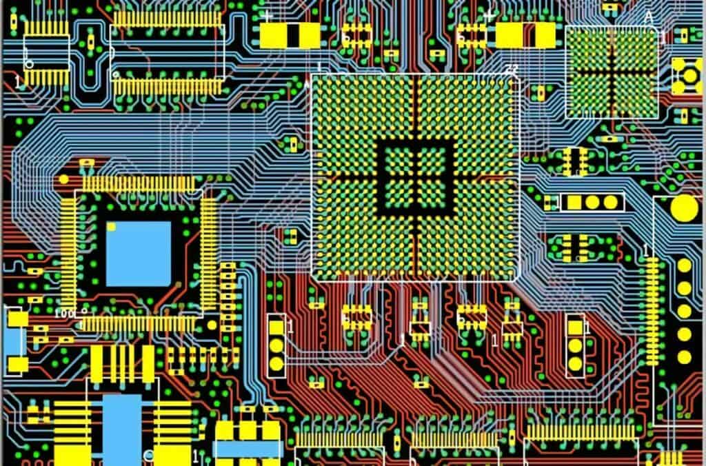
Floorplanning a High Speed PCB
The greatest central processor IC should be positioned close to the board’s center because it usually needs to communicate with every other component there.
Smaller ICs that are directly connected to the core CPU can be positioned anywhere around the large IC. This helps to keep the routing between the components as short and direct as possible. After that, peripheral components may be soldered onto the board in various locations to complete the functionality that is required.
You can set up your PCB design tools and begin routing your design when the components have been inserted. This is a delicate area of the design of a high speed digital circuit because bad routing might destroy signal integrity.
Signal integrity is much simpler to achieve, though, if prior processes were correctly carried out. To maintain managed impedance during routing, you should set your impedance profile in your PCB design guidelines so that any routes in the design are routed with the appropriate width, clearance, and spacing.
Routing, Signal Integrity, and Power Integrity
Designing your board with a specified impedance value in mind and maintaining it throughout the high speed layout and routing are the first steps in ensuring signal integrity. These are some other ways to guarantee signal integrity:
- In order to assure high-speed signals, try to take shorter pathways between components.
- Try to use as few vias as possible for routing; ideally, an internal layer should only have two vias.
- Backdrilling can be used to get rid of stubs on high-speed lines (such as 10G+ Ethernet).
- Look at datasheets to check if on-die termination is present; pay attention to the necessity for any termination resistors to prevent signal reflection; and with your fabricator about which materials and procedures can assist you avoid fiber weave effects.
- For your circuit board layout, use a crude crosstalk estimate or simulation to determine the right distance between nets.
- Keep track of the buses and nets that need their lengths matched so that tuning structures can be used to remove skew.
These crucial principles can be encoded as routing tool design rules, ensuring that you adhere to high speed design best practices.
