When it comes to PCB component testing, it’s an important requirement in PCB manufacturing sector, and it’s no laughing matter. However, it’s essential to understand that it can be tedious and intricate. Additionally, with the proper knowledge and tools, you can test your PCB components like a pro. We’ll discuss all the ins and outs of testing components, from the standard parts that require testing to the tools and techniques used to test them. So, whether you’re a novice to PCB component testing or a seasoned pro, let’s get testing and have a few ‘board’ laughs along the way!
PCB Component Testing
PCB component testing is fundamental in PCB manufacturing. It looks at certain standards of the board. The component testing reveals whether they meet the criteria to its specification. Therefore, this process gives assurance to the end customers about the product’s integrity.
Standard PCB Components That Require Testing
The following are the most common components you are likely to find on a printed circuit board:
1. Capacitors:
Capacitors are passive PCB components that store energy between two metal plates separated by a dielectric substance in an electric field. Capacitance depends on the plate’s surface area, the dielectric constant, and the distance between the plates. Capacitors are applicable in various electronic circuits and have numerous uses, including decoupling, timing, filtering, and smoothing. Typical capacitors include electrolytic, ceramic, tantalum, and film capacitors.
2. Inductors:
Inductors are passive circuit components that store energy in form of a magnetic field produced by a current traveling through a wire coil. The inductance of an inductor can vary depending on the number of coil turns, the coil’s diameter, and the core material. Inductors apply to various PCBs and electronic circuits and have numerous uses, such as filtering, tuning, and energy storage. Multiple inductors exist, including air-core inductors, ferrite-core inductors, and toroidal inductors.
3. Resistors:
Resistors restrict the flow of current in a PCB. The resistance depends on the resistor’s material, length, and cross-sectional area. Resistors are helpful in various electrical circuits and have numerous uses, such as voltage dividers, current limiting, and biasing. Some of the most common resistors include metal film, carbon composition, and wire-wound resistors.
4. Microchips:
The microchips are ICs (integrated circuits) comprised of millions of electronic components on a single piece of semiconductor material, including transistors, diodes, and capacitors. Microchips are helpful in various electronic products, including mobile phones, computers, and televisions. Microchips include microprocessors, microcontrollers, and memory chips, among others. Microprocessors are suitable for devices like computers and cell phones that require complicated computational activities.
5. Transistors:
Transistors are active components that amplify or switch electronic signals. Semiconductor materials, such as silicon, are helpful during the creation of transistors, which can be either bipolar or field-effect. The performance of a transistor depends on such factors as gain, frequency responsiveness, and power handling capability. In various electronic circuits, transistors are helpful for amplification, switching, and voltage regulation, among other applications. Bipolar junction transistors (BJTs), field-effect transistors (FETs), and insulated-gate bipolar transistors are common types of transistors (IGBTs).
6. Diodes:
Diodes are passive components that let current flow in a specific direction and blocks flow in the opposite direction. Standard and specialty diodes, such as Zener diodes and Schottky diodes, comprise semiconducting materials like silicon. Diodes are applicable in various electronic circuits and have numerous applications, including rectification, voltage regulation, and signal modulation. Rectifier diodes, Zener diodes, and light-emitting diodes are examples of common diode types (LEDs).
Tools for testing PCB Components

When testing for the functionality of the components of a PCB, you will require the following tools:
- Magnifying Glass:
The intention of this tool is to inspect the component to ensure is no visual damage or defect. Cross-cheking the elements and how they attach to the Printed Circuit Board helps ensure everything operates correctly. Additionally, a magnifying glass can easily detect burnt components, broken parts/connections, or signs of corrosion. It is possible to identify possible problems in advance and have them fixed before worsening.
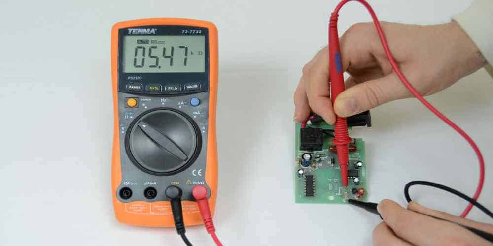
- Analog/Digital Multimeter:
A multimeter is essential for testing PCB components such as resistors, capacitors, and inductors. It measures alternating and direct current, voltage, resistance, and other parameters. This tool helps test whether a component is functioning correctly and diagnose problems. Furthermore, the device measures the quality of connections between the components and the PCB.
Techniques for Testing PCB Components:
We can perform PCB component tests through any of the following methods:
1. Automated Optical Inspection (AOI):
AOI is a non-contact, automated testing method that checks PCBs for flaws using cameras and image-processing software. AOI aids in testing solder joints, component positioning, alignment, and detection of faulty or missing components. The AOI system scans the PCB and finds any differences by comparing the images to a reference image.
Benefits of AOI:
Fast and efficient
non-destructive and without contact
high consistency and precision
Can identify a wide range of problems.
AOI’s drawbacks include the following:
Limited capacity to identify specific flaws, such as electrical shorts or open circuits.
It needs a comparison reference image.
high expenditures for initial setup and upkeep
2. In-Circuit Testing (ICT):
ICT (in-circuit testing) evaluates PCB parts that involve sending electrical signals to the board and observing how it reacts. Individual component testing and short-circuit detection frequently involve the use of ICT. The ICT system applies electrical signals to the PCB using a bed of nails or a fixture, and a testing program compares the measured values to the intended values. ICT is a quick and accurate way to test PCBs, although setting up the test fixture can take some time.
Benefits of ICT:
It may identify various flaws, such as open and short circuits.
Precise and effective.
Can you test individual parts?
Disadvantages of ICT:
Requires a test fixture, which can be time-consuming to set up
Limited ability to test passive components
Cannot test components that are not accessible from the surface of the PCB
3. Visual Inspection:
This method is a manual approach to testing PCB components that entail visually looking for flaws in the PCB. The visual inspection makes defects like missing or improper components, soldering flaws, and physical damage easy to identify. However, visual examination can be labor- and time-intensive, requiring magnifying glasses, microscopes, or cameras.
Benefits of visual examination:
Low cost and easy to complete.
Can identify a variety of defects.
Useful for both preliminary and comprehensive inspection
Negative aspects of visual inspection:
both labor- and time-intensive
limited capacity to identify some errors, such as internal flaws or flaws in secret places.
Possible operator error.
4. X-Ray Inspection:
This technique is a non-destructive testing method that examines PCB components with X-rays to check for flaws. BGA (Ball Grid Array) and other surface-mounted components that are challenging to inspect using different techniques are easy to examine using X-ray inspection. In addition, x-ray inspection can help check multi-layer PCBs and find internal flaws such as soldering, voids, and cracks.
X-ray inspection benefits:
Non-destructive
can identify underlying flaws and flaws in concealed places.
High resolution and accuracy
The drawbacks of X-ray inspection include the following:
High expenditures for initial setup and upkeep
limited capacity to identify specific sorts of flaws, such as open circuits.
Needs particular knowledge and experience.
5. Flying Probe Testing (FPT):
Using robotic probes, Flying Probe Testing (FPT) applies electrical impulses to the PCB and measures the response. It is a non-contact, automated way of evaluating PCB components. It is suitable for testing prototypes, low-volume production, boards with intricate or fine-pitched components, and low-volume production in general. FPT can be expensive for high-volume production even though it is a quick and effective way to test PCBs.
Advantages:
Non-contact and non-destructive.
Able to test Boards with complex or fine-pitch components.
May be suitable for prototype testing and low-volume manufacturing.
FPT disadvantages:
Costly for large-scale production
Testing passive components is difficult.
Only test components that are reachable from the PCB’s surface.
6. Functional testing:
Functional testing is a technique for evaluating PCB components that entails conducting functional tests on the PCB to ensure it complies with the desired standards. Complex or special PCBs and those designed for mission-critical applications are easy to test using functional testing. Functional testing involves emulating the PCB’s actual operating circumstances and ensuring it functions as intended.
Benefits of Functional Testing:
Able to test complicated or custom PCBs.
Can confirm that the PCB functions as anticipated under real-world operational circumstances.
Mission-critical applications are possible to achieve.
Functional testing drawbacks include:
costly and time-consuming
limited capacity to find specific flaws, like electrical shorts or open connections.
Needs particular knowledge and equipment.
7. Burn-In Testing:
The Burn-In Testing is a technique for evaluating PCB components that entails putting the PCB under a lot of stress for a long time to find any flaws that would not be visible under normal operating conditions. Burn-In Testing frequently helps test PCBs for high-reliability applications and components designed for relatively critical applications. During a burn-in test, we must expose the PCB to high temperatures, high humidity levels, or high voltage settings for a sustained time. We then evaluate the response.
Benefits of burn-in testing include:
It can find flaws that may not be visible during regular operations.
The technique can apply to high-reliability and mission-critical applications.
It gives a gauge of the reliability of the PCB under stress situations.
Disadvantages of Burn-In Testing:
Time-consuming and expensive
It cannot detect certain defects, such as open circuits or electrical shorts.
It requires specialized expertise and equipment.
Benefits of Testing PCB Components
Testing PCB components comes with the following merits:
1. Time Savings:
Saving time is one of the main advantages of PCB component testing. It is simpler to spot and address potential problems when you perform testing early in the PCB manufacturing process. This action helps to save time and drastically shorten production time. On the other hand, improper PCB component testing could lead to mistakes or faults we would quickly discover once the manufacturing process was over. Correcting these mistakes or flaws could take more time and cause manufacturing delays.
Moreover, PCB testing has grown increasingly automated as a result of technological advancements, which have sped up and improved the procedure. Automated testing eliminates errors, improves accuracy, and enables more thorough data analysis.
2. Cost Reduction:
Testing PCB components also aids in lowering the PCB’s overall production cost. For example, early-stage production problem detection and repair are less expensive than late-stage manufacturing defect repair. Also, finding and fixing mistakes earlier in the testing process is less costly than waiting until the product is on the market. Also, the price of PCB testing has fallen dramatically because of automated testing. Automated testing speeds up testing, lowers labor expenses, and limits human mistakes. As a result, it aids in reducing the overall cost of production and raises the end-user price point of the product.
3. Less Returned Goods:
Another benefit of PCB components testing is that it minimizes the quantity of returned goods. A PCB board may contain flaws if we do not adequately inspect it; it could cause the finished product to malfunction. Customer discontent returns and lost sales could occur if the product has flaws or needs to meet expectations. However, the possibility of returns considerably decreases by ensuring you’ve checked the PCB components and adhered to the requirements.
4. Greater Safety:
Testing PCB components also guarantees the safety of the finished product. A PCB board’s faulty or damaged components can produce product malfunctions that could injure the user or damage the environment. For instance, a PCB board that controls a medical device could malfunction and cause severe harm or even death. Hence, by testing the components of the PCB board, producers may ensure that the finished product is safe for usage.
5. Improved Quality:
Testing PCB components also help to raise the overall standard of the finished product. Manufacturers may guarantee that the finished product satisfies the necessary quality standards by identifying and fixing flaws in the early production phases. This feature improves the product’s performance, dependability, and longevity. Additionally, testing gives manufacturers information and insights that they may utilize to enhance product design and manufacturing, producing future products of even higher quality.
Conclusion
In conclusion, testing PCB components is a crucial step in producing PCBs. Testing ensures the product’s reliability, quality, and safety. Automated testing methods, including AOI, ICT, and X-ray Inspection, have sped up and improved the testing process. Moreover, testing prevents product returns and saves time and money. Thus, please don’t skimp on PCB component testing because it’s an essential step in the procedure. Although the process can be difficult and time-consuming, it is worthwhile. After all, why chance using a broken PCB when you can get it checked out to make sure it’s in working order? Besides, it’s much more fun to find out that your PCB works perfectly than it is to find out it doesn’t. So, if you’re ready to build a PCB, don’t forget to check your components first, or you might be in for a shocking surprise!
