The substance that houses the semiconductor device is referred to as the “IC packaging.” This package is indeed a casing that protects the circuit material into prevent corrosion as well as physical damage as well as to make it possible to place the electrical connections that link it to the PCB.
Because there are several distinct types of integrated circuits, there are numerous types of systems IC packaging to take into consideration. This is because various circuit designs would have had various requirements for the outer casing.
IC Packaging: Why Is It Important?
The fabrication of the semiconductor devices concludes with IC packaging. During this crucial stage, the package is placed over this semiconductor block into shield the IC from potentially harmful external elements as well as the corrosive environment.
This package is simply an encasement created to safeguard the block as well as to support the electrical connections that transmit signals to an electronic device’s circuit board.
Ball grid array packages were originally used by electronics packaging firms in the 1970s, but the technology for IC packaging has advanced since then. This plastic quad flat packs as well as the thin compact outline package were two more recent possibilities in package technology that supplanted pin grid arrays packaging at the start of the twenty-first century. Even as 2000s went on, companies like Intel helped to bring inside the land grid array packaging area.
Flip-chip BGAs, which provide larger pin counts compared to other types of package, replaced BGAs. Instead of only the edges, the FCBGA has output and input signals across the entire die.
IC Packaging Types
IC packaging comes in around 10 different varieties. Nonetheless, we’ll mention four in this post.
Through-Hole Mounting IC Packaging
For electronic components, the IC packaging serves as a mounting framework. Moreover, they call for the usage of lead on the components that fit into the drilled holes on the PCB.
They also bind to pads onto the backside. And this occurs by employing automated insertion mount equipment. Or by employing manual assembly that involves hand placement.
For items that can’t be mounted on a surface, this through-hole mounting package is perfect. Large transformers and heatsink power semiconductors are two examples.
Surface Mounting IC Packaging
Electrical components are installed directly onto the exterior of the PCB using a technique known as surface mounting IC packaging. Surface-mount devices include all electric devices which employ this IC packaging technique.
Moreover, this through-hole mounting IC packaging was absorbed by Surface mount package technology. How did this turn out to be the case? That was because, the SMT encouraged more automated production. Also, it enables cost-cutting and quality enhancement.
But this isn’t all. This surface-mount package features a platform which allows the installation of more components in a given space.
Chip-Scale IC Packaging
Chip-Scale IC packaging is another term for Chip-Scale packages. It got its moniker since it’s among the very few packages available in the chip size.
But this isn’t all. Any IC packaging must fulfill the following requirements in order to be classified as chip-scale:
- Be single-die
- Possess a direct surface-mountable package
- Having a space that is less than 1.2 times compared to the die’s size
The aforementioned idea was first out in 1993 by Hitachi Cable’s Gen Murakami as well as Fujitsu’s Junichi Kasai. The first idea demo, however, was made by Mitsubishi Electric.
However, there’s more.
The following are needed for chip-scale technology:
- The die must first be held by the interposer, which is where pads or balls are created. And the technique of a flip-chip BGA packaging is comparable to this IC packaging.
- The pads can also be etched or printed directly in the silicon wafers. And as a result, the packaging virtually matches the silicon die’s size.
- The water-level chip-scale packaging is the ideal illustration of this kind of packaging.
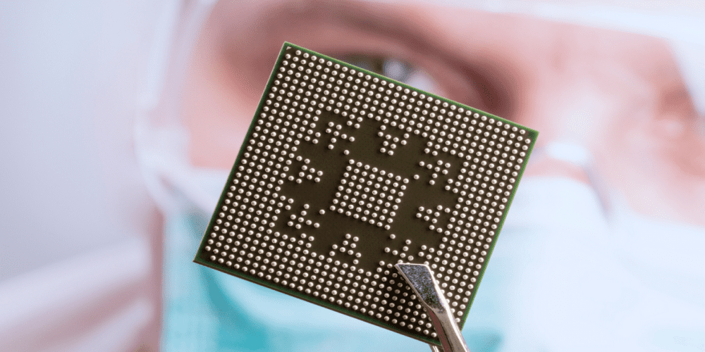
Ball Grid Array
Microprocessors are mounted permanently using a form of packaging called a ball grid array. Moreover, the package offers more connectivity pins compared to the dual or flat in-line package.
The best feature of such a package is therefore that you may use the full bottom area rather than just the perimeter. Also the traces that connect to a package lead to the wires or balls.
The die is connected to often shorter, perimeter-only packages via these wires or balls. As a result this package results in increased speed and improved performance.
Furthermore, as engineers, you must have exact control while soldering BGA chips. And the reason for this is because its mechanism is extremely fragile. Therefore, majority of companies usually work with automatic processes to prevent any errors.
Flat Packaging
Between two and four terminals rows are positioned around the borders of an integrated circuit in flat IC packaging. These packages are often surface-mounted, with leads either having an L- or J-shape as well as being completely missing, where such case they’re referred to as leadless terminals. Widely known flat pack IC packaging include: Quad Flat Packaging ,Thin Quad Flat Packaging (TQFP package), Small Thin Quad Plastic Flat Packaging, FQFP, plcc ic package, smd ic package, Low profile Packaging, Very-small Quad-flat IC Packaging), bga ic package, ceramic package ic, dip ic package, etc.
Surface Mounting vs. Through-hole Mounting

Two forms for IC packaging are often used, as was already mentioned: surface mounting and through-hole mounting. Here are the important aspects when comparing both of them.
Size: Large components are needed for through-hole mounting of a package. There is a significant variation in the sizes for ICs on the plated-through hole Boards compared to those with SMT. SMT enables reduced PCB sizes, hence ICs are smaller and more compact than in the plated through-holes.
Surface mount is preferable to the through-hole when size is an issue when packing your ICs. Since this surface mount seems small, you may also conserve space.
Component Density: As opposed to through-hole IC packaging, surface mount form of IC packaging offers greater component densities. With the surface mount, everything may be functionally installed in a considerably smaller area. Whenever it relates to through-hole, whereby components frequently are, such is not the case.
For example, numerous 16 or 14-pin in-line dual processors which are roughly 0.80 inches by 0.35 inches can precisely fit inside a region of a square inch and smaller. On the opposite, this would have been impossible if it had been plated thru-hole IC packaging.
Materials used in IC packaging
Semiconductors, ceramics, glasses, metals, composites, and polymers are some of the several materials used in this. Polymers function as conductors, whereas glasses and ceramics function as dielectrics or insulators.
On the contrary, metals function as conductors inside the package. These composites are made up of a variety of materials which can act as thermal enhancers or electrical conductors.
Patch material for IC packaging
You will need to employ to produce fixes if you discover yourselves in this kind of position. A patch seems to be a piece of cloth used to conceal an unsightly hole.
You may utilize a variety of patching materials. Some of them may be used during IC packing. Yet, the piezoelectric material makes up a portion of an ideal material.
Sealant for IC packaging
The term “sealant” is frequently used when discussing IC packaging. What exactly are bonds, as well as what are some of their applications? An adhesive, as the name suggests, is a substance that people employ to seal whatever they desire to close. The main purpose of sealants would be to make sure that its sealing mechanisms are airtight or waterproof.
Sealants are required during the IC packaging because they prevent damage to the remainder of the IC from air or water. Bonds are compulsory for such reasons.
Among the best adhesives to utilize is silicone sealant. They are durable and excellent at preventing corrosion throughout the entire package.
How to Choose an IC Package Types
We must first emphasize the significance of appropriate packaging. ICs must remain in their original packaging to facilitate easy handling as well as assembly on Boards. In order to prevent corrosion and damage, choosing the proper package is crucial. How are you going to select the appropriate IC package types?
The quantity of I/Os
The first consideration when selecting a package is the amount of I/Os. Due to their large pin counts, BGAs excel in this regard. However, this QFN package would be perfect for you if you’re looking for lower pin counts.
Heat control is the second thing you should think about. ICs are typically lower in size today, however they also have more comprehensive solder masks in order to stop the leakage of the thermal and electrical components. Make careful to go through the capabilities with the PCB provider. As a result, they’ll probably create too much heat, which is why thermal management is important. Nonetheless, BGAs frequently exhibit efficient heat dissipation, therefore you might choose to choose them.
High-Speed I/Os
Finally, take factors like High-Speed I/Os into consideration when selecting your IC package. You never want to compromise the package’s ability to link the I/O signals of the integrated circuits. Employ flip BGA for the greatest high-frequency signals.
PCB assembly is important. Can you get your IC packaging assembled in the quickest amount of time? Make sure to account for this upfront because not every service can meet your needs.
Design Considerations for IC Packaging
Knowing the technical information regarding the numerous design aspects that go into making IC packages is the first step in selecting the best IC package that suits your needs. For example, you should be conscious of the right substrates and material compositions for the IC packaging. Understanding the distinction between tape and rigid packaging substrates is also crucial.
Several businesses also think about employing laminates as alternatives to lead frames then choose substrates that are compatible with the metal conductors.
Composition of the Material
The IC package’s performance is substantially determined by its chemical, material, and electrical composition. Despite the functional differences, the lead-frame as well as laminate packaging both rely substantially upon material composition. This standard format, lead-frame packaging, has either gold or silver wire-bond finishes that are applied by spot plating. Because of this, the procedure is easier and less expensive.
Because of its compatibility with an underlying material, Alloy 42 is frequently used on the ceramic packaging. Since it protects the solder junction and provides conductivity, these copper lead frames are preferred for plastic packaging.
The material also serves as an important consideration for surface-mounted plastic containers due to laws in some regions.
This lead finish remains the subject of significant attention on next-level package assembly due to adjustments in European regulations. The goal has been to identify workable substitutes for the tin-lead solders that are simple to use and has historically been a standard in the industry. In part due to intense rivalry among suppliers, manufacturers have failed to coalesce behind one solution. It’s doubtful that the lead problem will get better on its own for a while.
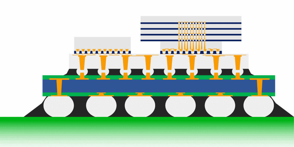
What Does Die-Attach Material Mean?
There are two main use for this particular IC packaging type. The initial objective is to protect your die from harm that outside forces could inflict. The second involves the redistribution of the output and input into a manageable and good fine pitch.
The packaging also has a defined structure that correctly guides the heat route away from the stacked die. This construction is more error-resistant and more suitable for the electrical tests overall.
The die-attach materials seem to be either liquid or film-based compounds that manufacturers use to prevent outgassing, which might reduce the integrity of the wire connection. Moreover, these materials operate as the stress buffer to prevent die breakage in the event that the CTE and substrate are not perfectly aligned.
There are several techniques for applying these die-attach materials, with certain methods being more complex than others. Die-attach is often used on assemblies when a wire bond occupies the surface face. Die-attach materials always seem to be thermally conductive.
Die-attach add electric conductivity to some assemblies. Manufacturers often try to avoid voids in a material to prevent the spots from becoming excessively hot in addition to the die. Both film and liquid die-attach materials may withstand outgassing and shield dies from harm.
Procedures for IC Packaging
These thinned wafers have been put into the middle of the release tape attached to the steel ring during the wafer dicing, exposing the active surfaces. From one magazine to the other, automated machinery batches-processes the wafers which are centered on a release tape and places them inside the center of a steel ring. The wafer saw’s input receives this output magazine out from a taping machine at this stage.
This wafer saw, which consists of the blade having diamond particles embedded in it and rotates at an extremely high speed, runs via the wafer and at saw streets that are constructed during wafer manufacture. This dicing machine can be configured to move a saw blade via the saw street at a set spindle speed, depth, and saw rate, dividing the wafer to individual dice.
The wafer’s surface is continuously rinsed with deionized water during the dicing process to keep it free of sawdust that can obstruct processing or result in faults.
Die bonding
According to their intended purpose, die go from the process of wafer saw to the die bonding. Based on the kind of packaging to be manufactured, each separated die were taken off from a release tape then affixed to the carrier frame made of alloy 42, copper, ceramic, palladium, or organic laminates. Leaded copper packaging are frequently used as illustrative examples in our article.
In the high-volume manufacturing plants of today, a frame could be single-site produced as one discrete unit all through the assembly as well as a combination of hundred pieces, batch-processed in order to gain economies of scale. This frame material may vary, however most HVM companies process units in batches that meet quality assurance and financial objectives.
Wire bonding
The die has become prepared to become electrically attached to a frame. A wire (usually gold) is thermosonically bonded to the die to achieve this. Wire bonding makes use of high-precision 3-D positioning software and equipment. Depending on the wire length, loop height of the wire, as well as the distance of the die-to-bond finger, etc., modern automatic equipment can bind 11 wires per second. According to the die size as well as intended purpose, the quantity of wire bonds or device might range between one and thousands.
Encapsulation
The IC packaging has to be protected by adding molded encapsulation after the wire bonding. Transfer molding is a widely used technique in which epoxy resin is liquefied under extreme temperatures and pressures and driven via the mold chase out over die frame and die itself as well as into the cavity upon that frame in which this die was previously positioned. The hardened epoxy creates the final package’s body.
Asides from transfer molding, integrated circuit could also be encased (or coated) inside the liquid epoxy that is cured so as to form solid coating around the integrated circuit. The encapsulant in this instance does not constitute the body of the package; rather, it just helps to safeguard the wires and die.
Managing time, flow, and pressure are important factors throughout the encapsulation stage. Miscalculations can result in a number of issues, including wire sweep (these are wires pulled together producing short circuits inside the component), incomplete molding, as well as mold voiding that are bubbles or pockets which forms inside the mold throughout the operation.
Lead finish
Throughout lead finishing, every copper leadframe gets cleaned and coated with lead/tin solder. The electrical charge applied to the leadframe causes lead and tin molecules to be drawn to and connected to a device as it moves through a succession of different electrolytic baths. The procedure regulates deposit concentrations, that change depending on the product’s requirements.
Marking
Following lead polishing and ball attachment, the portion is marked. An often step of branding or marking after molding is crucial to the whole process of assembly because it identifies the component for the quality assurance, dates the assembly, as well as establishes references to the assembly and wafer batches. The assembly’s bottom can accommodate the mark, freeing up the top for a marketing logo. Ink or laser are the two most basic marking techniques.
Today, laser marking is widely employed in the sector due to its excellent repeatability and quality. Cosmetic flaws and rework issues in ink marking might result in reduced yields.
Lead formation and singulation
Singulation, the removing individual parts from a matrix or strip, is the next phase in the manufacturing process for the laminate packages. Before singulation, a leadframe package normally goes through the lead shaping process.
Packing
This IC is currently almost finished. All that is left is the final quality check and packing in shipment trays, tubes, as well as automated tapes. The finished component went through up to 150 processes, some of which were highly automated. Depending on the materials, purpose, as well as product design, the entire procedure could take anywhere between 2 and 5 days.
Benefits and uses of IC Packaging
In almost all the electronic circuits, IC plays a number of crucial tasks. They handle all of the data processing and calculations. Among the most important components of data storage is IC. The electronic circuit like PCB cannot function as planned without ICs.
IC packaging has a number of noteworthy advantages. For instance, the IC packaging guarantees the component’s defense against deterioration and damage. Additionally, it ensures that this system as a whole receives a proper current flow.
Additionally advantageous is the IC packaging, which functions as a means of the “spreading apart” connections that result from the IC die’s tight pitch. The box disperses these mechanisms into areas with wide pitches, as required by the majority of PCB producers.
Conclusion
It’s essential to keep up with IC packaging trends. In the market of IC packaging materials, you can do this to maintain your competitiveness and make smart investments. Different market groups have an impact on the cost, acceptance, and accessibility of IC packaging materials. In addition, regional patterns may have an impact on whether or not packaging materials have been employed more or less frequently in specific parts of the globe.
