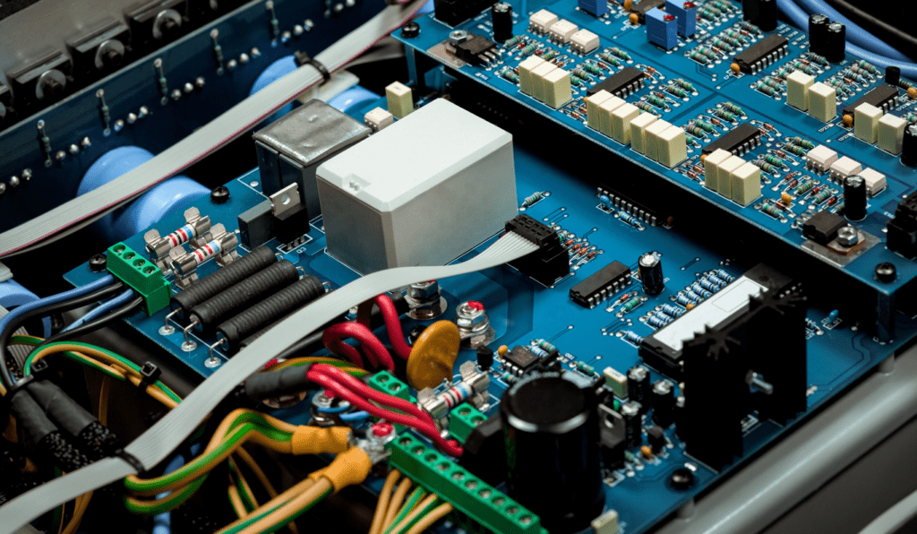
Printed circuit boards (PCB) and ancillary electronics are the focus of Meiko Electronics Co., Ltd.’s operations. It conducts its daily business via the following departments: Electronics Manufacturing and the Printed Circuit Board (PCB) Industry. The PCB Business provides electronic manufacturing services, including solder stencil design and fabrication.
Instruments used in industry and photography can be found in the array of products sold by the Electronics Business. The company also manufactures testing and inspection tools. The business began on November 25, 1975, and its headquarters remain in Ayase, Japan.
Meiko offers a vast array of services, such as PCB layout and fabrication, components mounting and integration, and the creation of a comprehensive selection of mechatronics and solutions.
MEIKO PCB Business
The company offers cutting-edge products such as high heat removal Circuit boards and large electrical current PCBs, both of which can withstand challenging environments like those found in automobile engines and solar electric generators, as well as the ever-shrinking form factor of cell phones and other portable devices.
Circuit Designing at MEIKO PCB
Meiko’s cutting-edge CAD technologies provide rapid, accurate, and comprehensive planning of ideal wiring for a constrained area. The company can easily shift into mass production because it applies its production expertise thoroughly, beginning with the design phase.
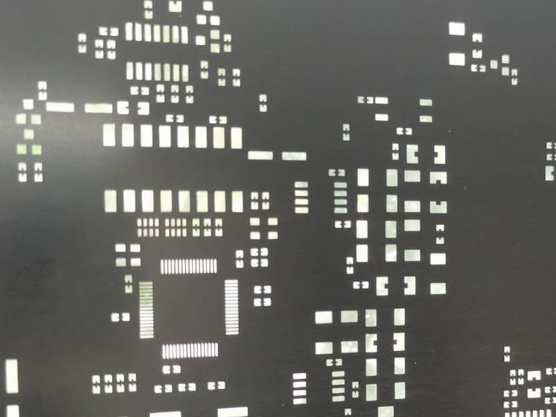
MEIKO PCB Solder Stencils
Meiko’s production facilities in Japan and elsewhere are state-of-the-art, so the solder stencils they supply are dependable, precise, and of high quality. Their metal masks are tried and true in many different industries, from mobile phones to autos to consumer electronics. Moreover, they have the fastest turnaround times in the business because of their streamlined production and sales process.
Electronic Manufacturing Services (EMS) of MEIKO PCB
Meiko offers a comprehensive service to assist their clients to succeed and adjust to the times. Pattern creation, manufacture, component procurement, assembly, testing, and shipping are all part of this service’s comprehensive outsourcing.
Electronics Businesses Of MEIKO PCB
Industrial Instruments
Inspection technology that checks the size and position of patterns and holes within a micron is crucial when dealing with PCBs made up of several components. Meiko’s PCB manufacturing experience allows them to supply PCB hole detection systems and electrical checkers.
Imaging Instruments
The image division at Meiko is responsible for creating and mass-producing cutting-edge video magnification hardware, software, and accessories such as matrix switchers and converters. Many people across the world, not only in Japan, utilize these items.
Research and Development System
Meiko’s R&D efforts are driven by the idea of “eco-friendly progress and cost-efficient technology,” which aims to reduce expenses while creating a new international benchmark. It’s possible to classify these pursuits into one of three broad groups:
- Creating cutting-edge products and supporting technology to meet the needs of the modern market.
- Future printed circuit boards (PCBs) and the technologies needed to make them economically viable require the development of new techniques.
- Technology for printed circuit boards (PCBs), including both current and future iterations and specialized variants
In addition to these efforts, they invest heavily in R&D to develop and implement technologies at each production site that is better suited to mass production, increase quality and reliability, reduce energy consumption, and better safeguard the environment.
The following is a review of the numerous types of progress.
· Embedded MEIKO PCB service
To further reduce the size of and improve the functionality of mobile devices, Meiko is creating built-in element techniques for fine-pitch electrode bear chips and small passive components. As the demand for automotive integrated power ICs has grown over the past several years, so has the number of research and development projects devoted to the design of components and simulation tools that can handle high electric currents and extensive heat production.
· Ultra-thick Copper PWB
Meiko has developed ultra-thick copper PWBs with the ability to apply high electric currents by creating a layered structure PWB with thicker copper film on wiring layers. Integrally manufactured PWBs are the subject of research and development to create PWB-forming technologies that allow for huge electric currents to be passed while maintaining a high level of reliability.
· PCB for millimeter waves at high frequencies
Meiko’s goal is to shrink and thin out PWBs by combining high-frequency circuits with control circuits. To accomplish this, there is a need of a combination of high-frequency materials such as LCP and Low-k Epoxy) and FR-4. More dense wiring is a goal for the company; thus, they are also working on the micro via-hole formation and multilayer high-frequency material development. As a bonus, they conduct their own tests to determine the quality of transmission and material qualities of novel high-frequency materials.
· Semi-additive HDI PCB
Wiring capacitance must be increased by increasing the number of wires between CSP electrodes from the current one to at least two since CSPs are likely to have increasingly thinner pitches and greater pin counts in the future. To do so, they need to develop technologies for manufacturing fine wiring with dimensions of L/S=40/40 m or smaller. As a result of these tendencies, the firm is working on copper foil semi-additive technologies to replace traditional etching methods.
MEIKO PCB Mdim-Based Technology
Meiko applies molecular junction technology to her fundamental research on Molecular Direct Metalizing (MDiM) through industry-academia-government collaborations. Metalizing of low dielectric material films to resolve metal adhesion issues and surface smoothing is now possible by the application of MDiM technologies, which allow for a molecular connection between an insulating material and a conducting material. Thus, MDiM technologies contribute to better high-speed transmission qualities.
Why Choose And Prefer MEIKO PCB?
· Technology Advancement:
Innovations frequently occur in the field. Companies like Meiko may expect this trend to persist for the foreseeable future. Businesses need to evolve alongside the rapid pace of technological change. Plus, as innovation in electronics continues, consumers will demand even more sophisticated tools.

· Manufacturing Capabilities:
The company’s headquarters and several production facilities are in Japan, indicating that it is capable of manufacturing. China is home to one of its manufacturing plants as well. This places them near their clientele and facilitates rapid, cost-effective production.
Conclusion
Meiko PCB has been successfully manufacturing products for many years. They’ve expanded greatly and come quite a distance since their infancy. Also, they are manufacturing goods on a global scale for their ground-breaking engineering.
As the number of people who utilize technology in their daily lives increases, this business is poised to enter a new era of increased popularity and wealth. Increased demand for phones and tablets will be to Meiko’s advantage.
