The electronics industry is intricate. In electronics designing and production, the use of abbreviations is common. Therefore, it is important one have an in-depth understanding of these abbreviations.
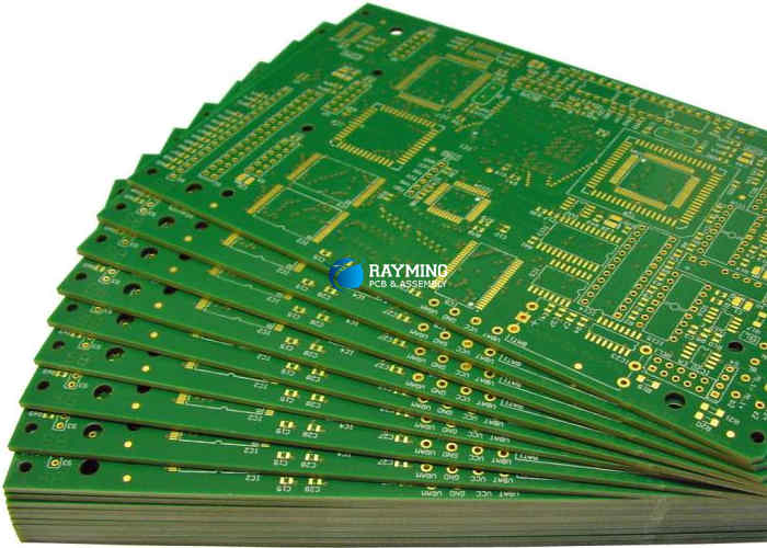
PWB and PCB are some of the most common terminologies in the PCB industry. There have been controversies as regards the meaning of PWB and PCBs. Since it is important to understand these two terminologies, we will have a comparison between them in this article.
What is a PWB Printed Wiring Board?
The full meaning of PWB is printed wiring board. Also, PWB features an epoxy glass substrate that creates interconnections to produce a circuit. In addition, a PWB comprises the production of an electrical network over a substrate. A PWB uses conductive paste to configure the arrangement of its circuitry.
The electrical connection is always designed on a conductive plate. PWB is a board on which manufacturers mount components and wire them. It is a board on which designers connect wires from point to point on a dielectric substrate.
PWB features no printed circuit on its board. PWB printed wiring boards are a designed substrate without components. The manufacturing involves etching away materials to have conduction-insulating surfaces between traces. Manufacturers connect the conductive layers on PWB by plated through holes. These holes help to install and electrically connect components.
What Does PCB mean?
PCB stands for printed circuit board. Also, it is a form of technology that enables the conductor to move from one side of the board to another side. Printed circuit boards are component-enabled. These boards already feature electronic components on their surface.
A PCB is a board that ensures the connection of electronic components. It is the foundation of any electronic device. This board features copper tracks that connect the holes where manufacturers place components. Printed circuit boards feature various electronic components.
Components on the Printed Circuit Board
PWB assembly features several electronic components. Asides from this, manufacturers mount these components on PWB printed wiring boards. The components on a PCBA include;
- Diode: This electronic component enables the free flow of current in one direction. Diodes have no resistance in one direction and high resistance through the other direction.
- Capacitor: The function of a capacitor is to hold an electric charge. It then discharges it when the circuit needs more power.
- Inductor: It saves energy in a magnetic field. This component stores energy that produces when current passes through it.
- Switch: This is a power button that regulates the flow of current in the circuit board.
- Resistor: This component resists current flow by discharging electric power as heat.
What is the Difference Between PWB and PCB?
PWB refers primarily to the board while PCB is the completed circuits on a board. People confuse PWB with PCB. However, it is important to understand there is a difference between these terminologies. There is a clear difference between these boards. While PCBs feature electronic components, PWB features none.
PCB is a board that features the entire circuitry. Furthermore, PWB is a board without any electronic components. This means that a PCB is a complete circuit board ready for installation on electronic devices. In addition, PWB is a term that explains the rudimentary manufacturing of the circuit board. The use of these terminologies varies according to different locations.
For instance, these terminologies are interchangeable within the electronics industry in the US. PCBs already have components on them. PWBs are the boards used for creating interconnections between these components. A PWB features holes for electronic components to pass through it. A PWB undergoes some chemical and physical procedures to become a full circuit board.
What is a PWB Circuit?
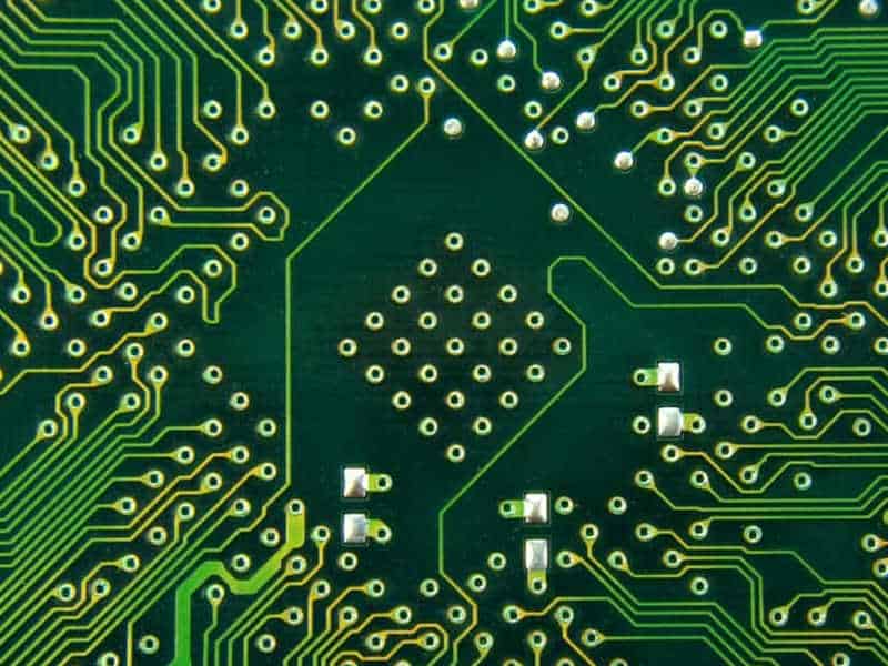
A PWB circuit is the foundation of almost all electronic products in the world. It is the surface on which manufacturers mount electronic components. The PWB circuit comprises different materials. A PWB circuit features non-conductive and conductive layers. The conductive layers are ideal for signal transfer within the circuit. The non-conductive layers are ideal for electrical isolation purposes.
Manufacturers use conductive layers like silver, gold, and copper for the fabrication of PWB. Copper is the most common and preferred material for PWB circuits. This is because of its good conductivity and low-cost properties. The conductive layer creates the path for the transfer of signal.
The non-conductive layer comprises materials that feature low electrical transferability. Also, FR-4, ceramic, and composite epoxy material are examples of materials used for the non-conductive layer. Manufacturers prefer FR-4 due to its dielectric properties.
The prepreg is another common material in PWBs. This material helps to hold layers together. Prepreg comprises fiberglass material with resin. Other materials such as solder are available in the PWB circuit. The solder material is a combination of tin and lead. Manufacturers use it to attach electronic components.
PWB Assembly
A PWB assembly is the board on which the manufacturer has installed all the electronic components on the circuit board. Furthermore, it provides a central hub to mount all the electronic components within a device. This assembly involves several steps. The PWB assembly gets rid of the short circuit and loses any connection via copper tracks.
PWB assembly consists of a number of components. You will find components like LED, battery, and diodes among others in PWB assembly. The fabrication of PWB assembly is a complex process that requires various steps.
The PWB is a printed wiring board with electronic components mounted on it. In a PWBA, manufacturers use soldering processes to attach components on the board. In addition, PWB assembly must be able to withstand both environmental and mechanical stress in a normal operation. A PWBA is a complete circuit board that has gone through component placement, soldering processes, and inspection.
PWB Assembly Process
The PWB assembly process involves different stages. Manufacturers need to perform these stages carefully to achieve a functional PWB assembly. It is important that you integrate each of these stages properly. Furthermore, you must consider the output to input results at every stage. This will help you maintain quality throughout the PWB assembly process. You would also be able to detect and correct errors at early stages.
Solder paste
This is the first stage for a PWB assembly. The manufacturer adds a solder paste to all areas that require soldering. You have to do this before mounting the components on the PWB. The component pads are the areas that need solder paste. The solder paste is a combination of flux and grains of solder.
The assembler places the solder screen on the PWB. A runner moves through the screen and deposits solder paste on the screen via the holes on the board. The assembler must control the amount of solder paste to ensure the joints have the appropriate amount.
Component placement
This is an important stage in the PWB assembly process. This stage involves the placement of components on the PWB. The electronic components are mounted on the PWB. Here the manufacturers solder the component on the surface of the board. In those days, this process was manual. Assemblers pick and place components on the PWB using a pair of tweezers. However, technology has improved a lot of things.
These days, PWB assemblers now use a machine to pick and place components. The machine automatically places the electronic components on top of the solder paste in preprogrammed areas.
Reflow soldering
Here, the solder paste must solidify. In fact, the solder paste and the mounted components must remain in place. PWB assembler achieves this through “reflow.” After the placement of components, the assembler transfers the board to a conveyor belt. This belt passes through a reflow oven. The oven is similar to that of a commercial pizza oven.
The reflow oven comprises various heaters. These heaters heat the wiring board to an appropriate temperature. The solder paste melts at this stage. The melted solder then passes through the cool heaters which cool down and solidify it.
Inspection and test
The inspection process of a PWB might take time, but it is worth the time. After you have completed all the assembly processes, you need to inspect the board. Thorough inspection helps you detect any defect or error in the PWB assembly. You can perform an automatic optical inspection on the printed wiring board assembly. This process detects poor joints, misplaced components, and more.
Aside from the automated optical inspection; there are other types of inspection. There is the visual inspection and X-ray inspection. Your PWB will also go through some tests.
PWB Types and Manufacturing Methods
PWBs are classified in several ways. In terms of overall complexity, the industry classifies them based on layer counts. According to layer count, PWBs are into three categories; single-sided, double-sided, and multilayer. There are over two layers of circuitry in a multilayer PWB. This means it features at least one layer in the substrate beneath the board’s surface.
A multilayer PWB may feature as many interconnected layers as possible. However, the common ones are 4, 6, and 8 layers. Double-sided PWBs feature only two interconnected layers. This PWB type is much easier to fabricate than the multilayer boards. The single-sided printed wiring board features a layer of circuitry.
Experts also categorize PWBs as their base materials. This board falls into three categories which are flexible, rigid, and rigid-flex. The flexible PWB comprises polyester and polyimide substrates. These boards remain flexible and are ideal for several applications. Flexible PWBs can bend into shape a few times. The PWBs can withstand many flexing cycles.
The second category is the rigid PWB. Manufacturers use glass-reinforced epoxy-resin to fabricate this board. The thickness of the rigid PWB is less than 0.1 inches. The rigid-flex PWB features the properties of both rigid and flexible boards.
As regards manufacturing methods, PWBs fall into two types. These are subtractive and additive processing. Subtractive processing involves removing copper selectively from a PWB to create a circuit. The manufacturer adds other metals during the plating process. The subtractive processing refers to using image transfer from an image file to a copper circuit on a board.
Additive processing is a method in which the manufacturer forms an image by adding copper. This process doesn’t involve any etching or copper removal. The additive approach has been used for the production of PWB for so many years.
Types of PWB Manufacturers
PWB manufacturing is a complex and technical operation that requires large equipment. The PWB industry designs PWBs for specific applications. This industry is a highly competitive one. The two types of manufacturers that produce PWBs are independent and captive.
Independent manufacturer
This type of manufacturer fabricates PWBs for use in electronic products. There is high competition among independent PWB manufacturers across the globe. These manufacturers compete with each other to get contracts from customers. They produce PWBs with the aim of delivering them in the open market. An independent manufacturer will bid on its ability to fabricate a product according to a customer’s specifications.
Captive manufacturer
The captive manufacturer is also referred to as Original Equipment Manufacturer (OEM). These manufacturers manufacture PWBs to design their own electronic devices. However, these manufacturers are few in the world today. These manufacturers don’t fabricate PCBs for sale in the open market.
Frequently Asked Questions
What type of surface finish can be used for a PWB printed wiring board?
Manufacturers use different surface finish options for PWBs. Surface finishes like ENIG, immersion tin, and HASL are ideal for PWBs.
Why is copper popular in PWBs and PCBs?
Both PWBs and PCBs feature copper. Copper is a vital material for the fabrication of PCBs and PWBs. This is because copper features great properties. This material is highly conductive and budget-friendly.
What are the applications of PWB printed wiring boards?
PWBs are ideal for use in most electronic devices. These boards are very vital in the electronic industry. They are used for the production of consumer electronics, medical devices, and more.
Conclusion
We have compared PWB vs PCB in this article. Both PWBs and PCBs are the foundation for most electronic devices. While there are differences between these two terminologies, they also have similarities. PCBs and PWBs provide support for different technologies and products in almost all industries. The fact is that the usage of PWB vs PCB varies across the world.
