Printed circuit boards (PCBs) are the backbone of modern electronics, and they are found in virtually every electronic device we use today. PCBs are used to connect and control electronic components, and they are often enclosed in a protective casing or enclosure. PCB enclosure design is an important aspect of electronic product design, as it ensures that the PCB is protected from environmental factors such as dust, moisture, and electromagnetic interference.
The design of a PCB enclosure must take into account a variety of factors, including the size and shape of the PCB, the type of electronic components being used, and the environmental conditions the product will be exposed to. The enclosure must also be designed to allow for proper ventilation and cooling of the PCB, as excessive heat can damage electronic components. In addition, the enclosure must be designed to allow for easy access to the PCB for maintenance and repair purposes.
Overall, PCB enclosure design is a crucial aspect of electronic product design, as it ensures that the PCB is protected and operates effectively in a variety of environmental conditions. A well-designed PCB enclosure can help to extend the lifespan of electronic products and reduce the need for repairs or replacements.
Key Considerations
When designing a PCB enclosure, there are several key considerations that must be taken into account. These include environmental factors, mechanical constraints, and electrical requirements.
Environmental Factors
One of the most important considerations when designing a PCB enclosure is the environment in which it will be used. This includes factors such as temperature, humidity, and exposure to dust and other contaminants. The enclosure must be designed to protect the PCB from these environmental factors, which can cause damage or malfunction.
To ensure the enclosure is suitable for the environment, it is important to consider the materials used. For example, if the enclosure will be exposed to high temperatures, materials with high thermal conductivity should be used to dissipate heat. Similarly, if the enclosure will be used in a dusty environment, it should be designed to prevent dust from entering the enclosure.
Mechanical Constraints
Another important consideration is the mechanical constraints of the enclosure. This includes the size and shape of the enclosure, as well as any mounting requirements. The enclosure must be designed to fit the PCB and any other components, while also being easy to assemble and disassemble.
To ensure the enclosure meets these requirements, it is important to consider the manufacturing process. For example, if the enclosure will be injection molded, it may be necessary to design the enclosure in multiple parts to facilitate the molding process.
Electrical Requirements
Finally, it is important to consider the electrical requirements of the enclosure. This includes factors such as grounding, shielding, and electromagnetic compatibility (EMC). The enclosure must be designed to protect the PCB from electromagnetic interference (EMI), while also providing proper grounding and shielding.
To ensure the enclosure meets these requirements, it is important to consider the materials used. For example, conductive materials such as aluminum or copper can be used to provide shielding, while non-conductive materials such as plastic can be used to prevent EMI. Additionally, it may be necessary to use filters or other components to reduce EMI.
Overall, when designing a PCB enclosure, it is important to consider environmental factors, mechanical constraints, and electrical requirements to ensure the enclosure is suitable for the intended use.
Design Process

When designing a PCB enclosure, it is important to follow a structured design process that includes conceptualization, prototyping, and testing. This process ensures that the final product meets the desired specifications and is functional, reliable, and manufacturable.
Conceptualization
The first step in the design process is conceptualization. This involves defining the design requirements, creating a design concept, and selecting the appropriate materials and components. It is important to consider factors such as size, shape, weight, and environmental conditions when designing the enclosure.
During the conceptualization phase, it is also important to consider the manufacturing process. The enclosure design should be optimized for manufacturing, which includes minimizing the number of parts, reducing assembly time, and minimizing the cost of materials.
Prototyping
Once the design concept is finalized, the next step is prototyping. This involves creating a physical prototype of the enclosure design using 3D printing or other prototyping techniques. The prototype is used to test the design for fit, form, and function.
During the prototyping phase, it is important to identify any design flaws or issues that may impact the final product. Any necessary design changes should be made at this stage to ensure that the final product meets the desired specifications.
Testing
The final step in the design process is testing. This involves testing the final product for performance, reliability, and durability. The enclosure should be tested under various environmental conditions to ensure that it can withstand the intended use.
During the testing phase, it is important to identify any issues or defects that may impact the performance or reliability of the product. Any necessary design changes should be made based on the results of the testing to ensure that the final product meets the desired specifications.
Overall, following a structured design process is critical when designing a PCB enclosure. By following the process of conceptualization, prototyping, and testing, designers can ensure that the final product meets the desired specifications and is functional, reliable, and manufacturable.
Material Selection
Selecting the right material for an enclosure is crucial to ensure that the printed circuit board (PCB) is protected from environmental factors and is able to function optimally. There are several factors to consider when selecting a material for the enclosure, including cost, strength, weight, and resistance to heat, moisture, and chemicals.
One of the most commonly used materials for enclosures is plastic. It is lightweight, affordable, and easy to mold into various shapes and sizes. However, it may not be the best choice for applications that require high strength or resistance to extreme temperatures or chemicals.
For applications that require high strength and durability, metal enclosures may be a better option. Metals such as aluminum and steel are strong, durable, and can provide excellent protection against environmental factors. However, they are generally more expensive than plastic and may require additional machining or processing to create the desired shape and size.
Another option for enclosure material is composites. Composites are made up of two or more materials that are combined to create a stronger, more durable material. They can be customized to meet specific requirements and can provide excellent protection against heat, moisture, and chemicals. However, they may be more expensive than plastic and may require specialized manufacturing processes.
When selecting a material for the enclosure, it is important to consider the specific requirements of the application and weigh the pros and cons of each option. By carefully considering all factors, it is possible to select a material that will provide optimal protection for the PCB and ensure that it functions properly for the intended lifespan.
Manufacturing
When it comes to manufacturing PCB enclosures, there are two main processes: fabrication and assembly. Each process requires specific techniques to ensure the final product meets the desired specifications.
Fabrication Techniques
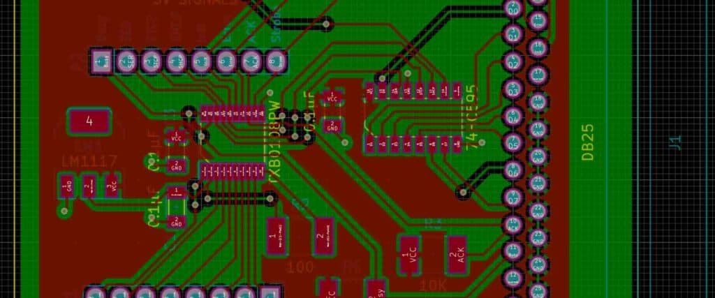
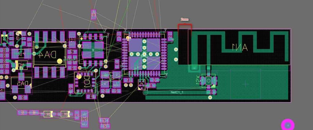
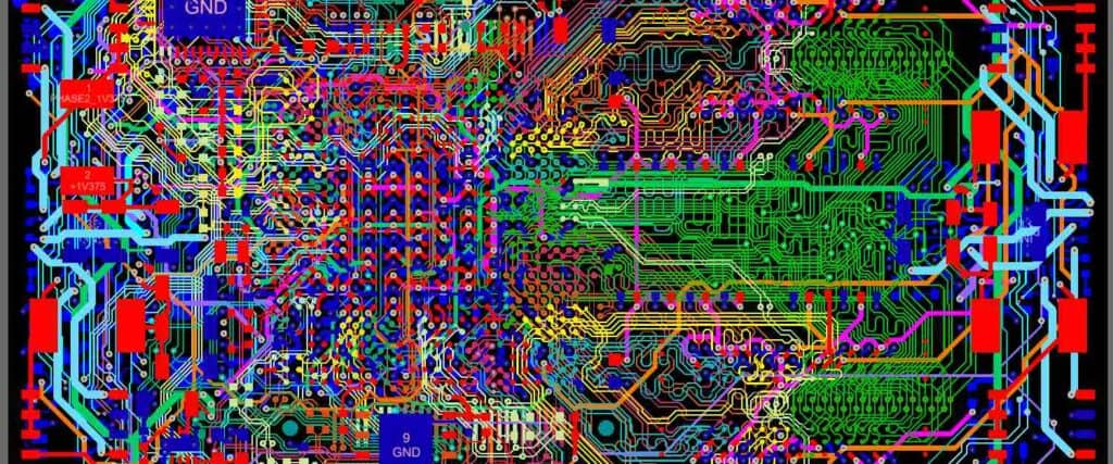
Fabrication involves creating the PCB itself, which includes the substrate, copper layers, and other components. There are several techniques used in PCB fabrication, including:
- Etching: This technique involves using a chemical solution to remove unwanted copper from the PCB substrate. The remaining copper creates the circuitry.
- Milling: Milling involves cutting the PCB substrate to create the desired shape and size. This technique is often used for small production runs or prototypes.
- Printing: Printing involves using a specialized ink to create the circuitry on the PCB substrate. This technique is often used for high-volume production runs.
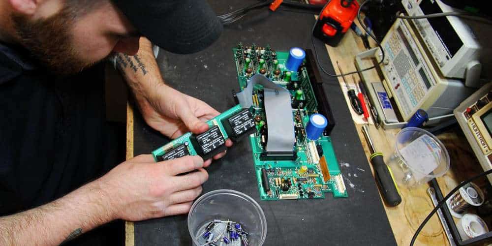
Assembly
Once the PCB substrate is fabricated, it needs to be assembled into an enclosure. This process involves attaching the components to the PCB and then enclosing it in a protective case. There are several techniques used in PCB assembly, including:
- Surface Mount Technology (SMT): SMT involves attaching components to the surface of the PCB using solder. This technique is often used for small components and high-density circuitry.
- Through-Hole Technology (THT): THT involves inserting components through holes in the PCB and then soldering them in place. This technique is often used for larger components and components that require a stronger mechanical connection.
- Wire Bonding: Wire bonding involves connecting components to the PCB using thin wires. This technique is often used for components that cannot be attached using SMT or THT.
In conclusion, understanding the different techniques used in PCB enclosure manufacturing is crucial to creating a high-quality product. By utilizing the appropriate fabrication and assembly techniques, manufacturers can ensure that their PCB enclosures meet the desired specifications and are suitable for their intended use.
Cost Optimization
When designing a PCB enclosure, cost optimization is a crucial factor that should be considered. Here are some ways to optimize the cost of your PCB enclosure design:
Material Selection
Choosing the right material for your enclosure can significantly reduce the cost of your design. Some materials such as aluminum and steel may be more expensive, while others like plastic and acrylic are more affordable. However, keep in mind that the choice of material should not compromise the functionality and durability of the enclosure.
Simplify Design
Simplifying the design of your enclosure can help reduce the cost of manufacturing. Avoid complex shapes and designs that require additional machining and assembly. Instead, opt for simple and straightforward designs that can be easily manufactured.
Standardization
Using standard components and parts can help reduce the cost of your enclosure design. Standard parts are readily available and can be purchased in large quantities, reducing the overall cost of manufacturing. Additionally, standard components are often more reliable and have a longer lifespan, reducing the need for maintenance and repairs.
Size Optimization
Optimizing the size of your enclosure can help reduce the cost of materials and manufacturing. Smaller enclosures require fewer materials and are easier to manufacture, reducing the overall cost of the design.
Manufacturing Process
Choosing the right manufacturing process can help reduce the cost of your enclosure design. Injection molding, for example, is a cost-effective way to manufacture plastic enclosures in large quantities. On the other hand, CNC machining may be more expensive but allows for more design flexibility and precision.
In conclusion, cost optimization is an essential factor to consider when designing a PCB enclosure. By selecting the right materials, simplifying the design, standardizing components, optimizing size, and choosing the right manufacturing process, you can reduce the overall cost of your design without compromising functionality and durability.
