It is important to inspect PCB manufacturing and assembly. Accurate inspection is of great importance in PCB manufacturing. There are different techniques for inspecting circuit boards. With the increasing demand for complex circuits, accuracy in PCBs is very vital.
Over the years, electronics production has become more sophisticated. The use of complex circuits in electronic devices made inspection a difficult process. However, with the introduction of X-ray machines, this process has been made easier. The X-ray PCB inspection is one of the reliable and accurate PCB inspection methods. We will discuss this inspection method and how it impacts the PCB industry.
What is PCB X Ray Inspection?
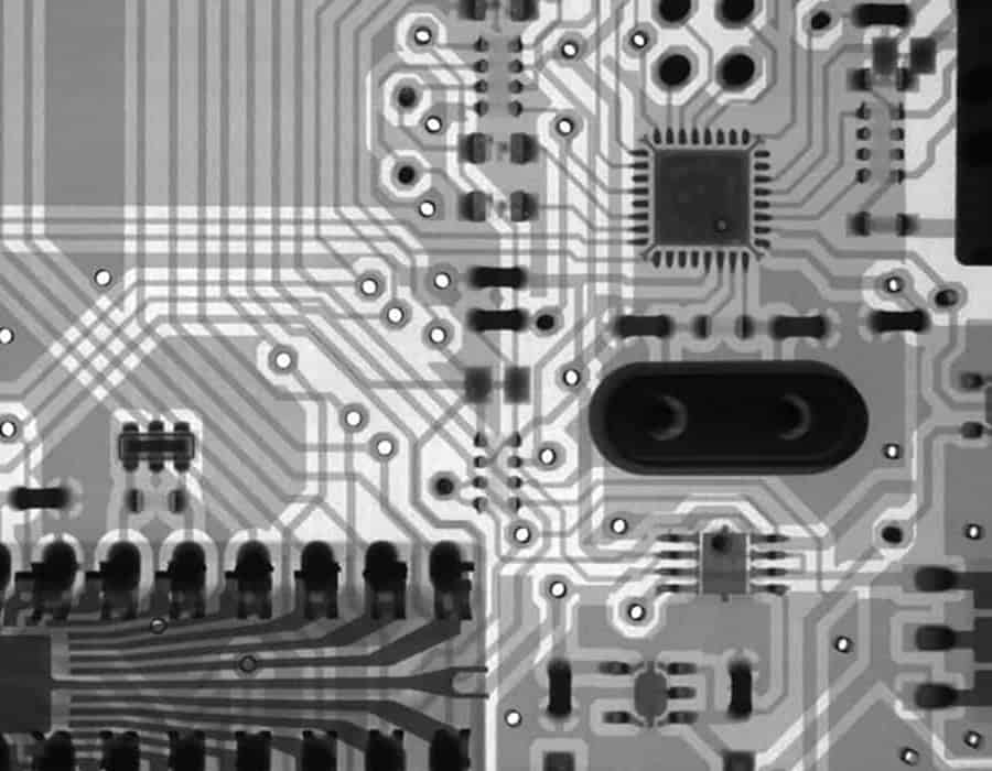
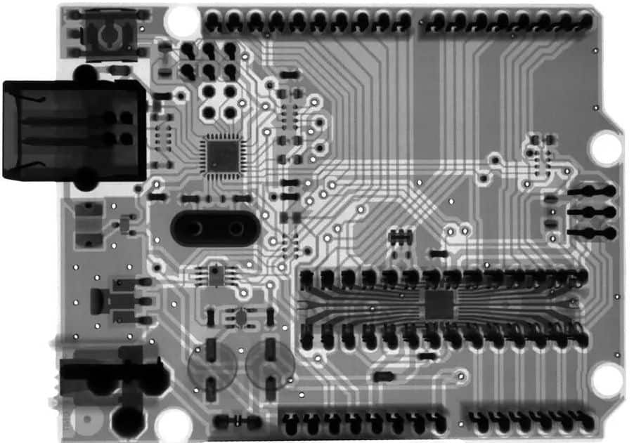
This is an inspection technique that uses an automated X-ray machine to detect hidden features within a target PCB. The X-ray machine is popular across various industries. From the aerospace industry to the medical industry, X-ray inspection is widely used. However, it has gained popularity in the PCB industry.
The PCB X ray inspection applies same principles as the automated optical inspection. However, PCB X ray uses X rays to detect errors. This X ray features strong electromagnetic waves. It also features a wavelength shorter than visible light. One great advantage of X-ray machines is that they have the ability to detect what visible light can’t. The automated X-ray inspection can detect hidden defects in solder.
Request X-Ray PCB Quote, Pls Send PCB files to Sales@raypcb.com Now
How does the PCB X Ray Machine Work?
The X ray machine helps to carry out PCB X ray inspection. It is important to understand how this tool works. PCB X ray machine comprises three features. The X ray tube, detector, and platform are these basic features. The X ray tube can generate X-ray photons. While the platform carries the sample in different directions. This enables it to inspect from different magnitudes and angles. The detector catches and receives x ray photons. It then transforms them into an image.
X-ray photons help the X –ray imaging function well. The photons are passed via a material and received on the other side. They pass through materials in a different way depending on their physical features. Heavier elements consume more X-ray photons. This makes it much easier to image. Since different materials act in a unique way, the X ray collects various amounts of photons.
PCB components feature heavier elements, which make them easily seen on an X-ray image. The PCB X ray machine can inspect the inner layout of the circuit board. This helps to evaluate the efficiency and detect faults in the PCB design.
The PCB designer places the component between the detection component and the PCB X-ray machine. Some factors determine the penetrating power of X-ray machine. These factors include material’s density and the energy of the X-ray.
Classification of X-ray Machine
There are different categories of the PCB X ray inspection systems. The classification of these systems is explained below:
3D system
This system can create 3D photos of a PCB by establishing a series of 2D cross-sections. A CT scan works in a similar way. 3D system works with laminography method. The CT method can work offline because of the complex algorithms incorporated. The laminography method is useful both offline and online.
2D system
This system shows the 2D photos from the two sides of the circuit board simultaneously. This creates a photo of the PCB components. The 2D system can work offline or online.
Offline operation
All x ray machines can carry out sampling inspection and panel inspection offline. Offline tools can run quickly. However, they are less cost-effective as the quantities of product increase.
Online operation
Some X ray machines function online for comparison and data collection purposes. This enables it to process more complex PCBs. But, online capability slows down the X-ray machine. This decreases capacity while increasing cost.
Principle of X Ray Inspection
The high penetrating power of PCB X ray machine is a very important feature. X rays have the ability to penetrate a substance that is invisible to light. PCB X ray machine produces light that can get to the test subject. This shows a photo with various densities and thicknesses. The photo quality sheds more light on the joint’s quality.
X ray materials take in X rays proportional to their atomic weight. The fact is all materials take in X ray radiation based on their atomic number and density. Generally, materials comprising heavier elements take in more X rays. Also, these materials are much easier to image. Materials that comprise lighter elements are more visible to X rays.
X ray inspection devices work based on the inspection principle. This principle is known as X ray projection microscope. In this process, an X ray launching tube passes through an inspected PCB. The X ray absorption varies in materials. This is due to the differences in atomic number and material.
Therefore, it is important an X ray inspection system has X ray photos. This will provide details in the process of defect analysis. This system must feature enough magnification to meet the present and future demands. X rays feature high-energy electromagnetic radiation. X ray photons feature energies within the range of 0.1 and 1,000 kV.
During the X ray inspection, the manufacturer places the component between the detection media and X ray machine. The energy of the X ray determines the X ray penetration. The detection media often generates a visual image of the component.
Common Defects X Ray PCB Inspection Detects
An X ray system can detect several PCB defects. It detects some faults an optical or electrical test will find difficult to detect. This is because of its high penetrating power. Below are some common faults X ray PCB inspection will find out.
Missing solder
This defect is problematic. It could include improperly placed solder on a PCB pad. Also, it could be a result of a missing solder ball on a flip chip or BGA. Rough handling of packages can make solder joint knock off. Electrical tests can also detect this problem. However, X ray inspection instantly detects the absence of solder.
Solder bridges
Solder bridges happen between two adjacent contacts. This is a result of one or both contacts receiving extreme solder. Solder bridges could also happen when solder sticks in the wrong place. This defect occurs on reworked PCBs since it is difficult to manually place solder on a PCB. X-ray image reveal bridges as dark patterns.
Open connections
This defect happens when contact and the solder on the pad don’t come in contact. For instance, the solder balls at one end of a BGA contact well, but the balls at another end don’t. An X-ray system can identify the unconnected balls. However, not all open connections reveal themselves in X-ray images. This system can find it difficult to identify hairline cracks that may result in intermittent connection in solder.
Component shift
This problem happens during reflow. A component shift is a result of the ability of components to float on molten solder. BGA components may rearrange themselves since the molten solder features a surface tension. However, these components will stay in their position in most cases. Therefore, manufacturers should place components right in the middle of the pad.
Request X-Ray PCB Quote, Pls Send PCB files to Sales@raypcb.com Now
Other Defects X ray Inspection can Detect
X ray inspection detects a lot of defects and failures in PCBs. However, the X rays help to inspect the Ball Grid Array Integrated Circuit. The BGA circuit is an SMD component without any leads. This SMD component incorporates metal spheres made of solder.
One of the most important defects PCB X ray machines detect is the BGA solder joint. The BGA X ray inspection involves the use of X ray to inspect BGAs. In Ball Grid Array circuits, solder joint defects are a big problem. Manufacturers can’t use optical methods to inspect BGAs. This is because solder joints hide beneath BGA components.
Furthermore, electrical tests can’t reveal the BGA’s electrical conductivity instantly. These tests can’t speculate the life span of the solder. BGA X ray inspection is the most reliable technique for inspecting BGA solder joint. This inspection checks the solder joint underneath the PCB components. The X ray inspection is popularly used for inspecting BGAs.
The BGA x ray inspection detects the faulty components and detaches them from the PCB. It does this by melting the solder joint. The BGA component undergoes serious heat until the solder joint melts. In this process, the manufacturer heats the component in a rework station.
This station has an infrared heater, a vacuum device, and a thermocouple. The vacuum device raises the package and the thermocouple regulates the temperature. The inspector must only heat the faulty BGA component. As the number of components on PCB increases, component placement becomes complex. BGA packages can help to manage this complexity.
BGA packages are popularly used in the PCB industry. These packages are ideal for compact electronics since they have more IO counts.
Types of PCB X Ray Inspection System
The X ray inspection system is in two categories. These categories are manual X ray inspection system and automated x ray inspection.
Manual X ray inspection system
In this system, the manufacturer inserts a circuit board into the system manually. Then the system generates an image. This system can take a photo of a portion of the PCB. Therefore, you select the area you want to work on and acquire the photo. The photo displays on the screen. You can get information about the metrology and the quantitative features about the photo.
A manual X ray inspection system can convert dimensional measurements into quantitative information. Some manual systems don’t analyze the X ray photo automatically. In this case, the operator must observe other PCBs to evaluate a board under inspection. Therefore, the inspector must be able to differentiate good connections from bad ones.
Automated X ray inspection
This type of system is ideal for high-volume PCB production. Automated PCB X ray inspection will meet your demands more than a manual system. The automated inspection can accept circuit boards from robotic handlers or cartridges.
In the automated X ray inspection, computer regulates the image-acquiring and board-loading steps. The computer may decide about quality based on the sophistication of the system. Therefore, it can make pass or fail decisions. Also, it can transmit test data for statistical analysis.
This system can’t take accurate X ray photos of the whole PCB at once. Then the computer positions the PCB and gets images automatically. After this, the computer analyzes the photo information. Then, it concludes if the board needs rework. You will need to train the system since it depends on a computer to carry out the inspection steps.
Advantages of X ray Inspection in PCB Manufacturing
X ray inspection helps to detect a lot of defects in PCB Manufacturing. It is of great importance as it helps to gain quality control in the PCB industry.
Improves PCB quality
PCB X ray inspection improves the quality of PCB production. This is because it can detect any failure or defect in PCB assembly on time.
High detection function
The X ray machine features a high detection function. This makes it detect what seems invisible to optical inspection. PCB X ray inspection can identify a lot of defects like solder joints and missing components. It can also detect defects that other methods can’t identify.
Higher test coverage
Most of the defects in PCBs are invisible to the human eye. The internal conditions of solder joints can change in the high heat soldering furnace. Hence, the human eye can’t see these problems. However, the X ray inspection can detect these problems.
Offers relevant measurement information
The X ray inspection equipment provides useful measurement information on the PCB. This information helps to evaluate the solder paste’s thickness on the PCB.
Conclusion
PCB X ray inspection is a powerful inspection technique in PCB production. Although there are other inspection techniques, X ray offers more benefits. This inspection can detect what visible light can’t. PCB X ray can penetrate substances that remain invisible to light. Due to its high penetrating power, it is considered the best inspection method for PCB.
