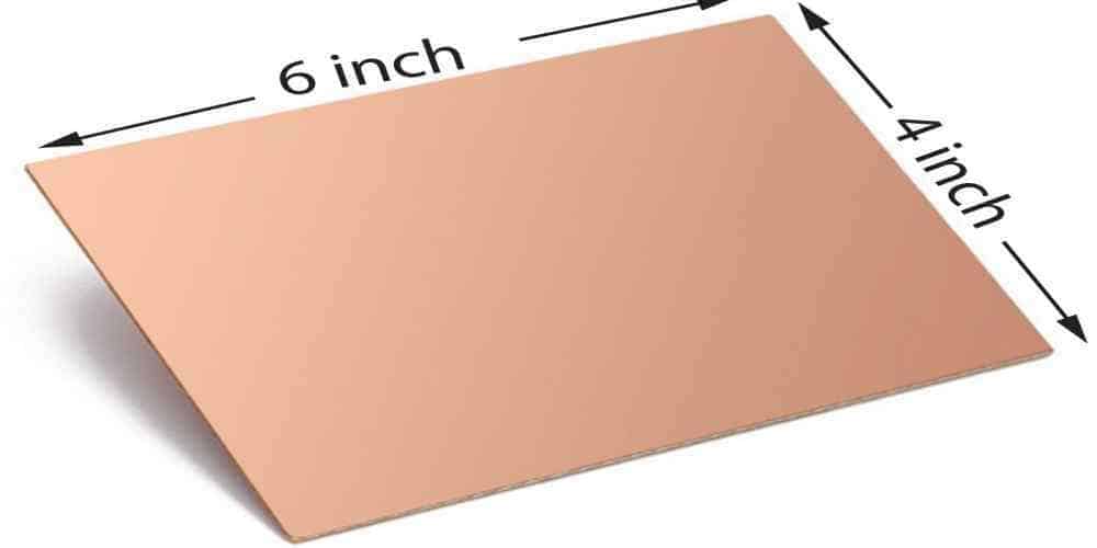
The other name for phenolic PCBs is FR-2 PCBs. These are a type of printed circuit board made from phenolic resin and paper or fiberglass. Manufacturers use them in low-cost applications where high-frequency operation is not necessary. Phenolic PCBs are a popular choice due to their affordability, ease of manufacturing, and good electrical insulation properties.
The history of Phenolic PCBs dates back to the 1950s. These were the first cheaper alternative to other PCB materials such as ceramic or fiberglass. Phenolic resin, a synthetic thermosetting polymer, was an effective substitute for these more expensive materials. Phenolic PCBs quickly became popular for their affordability and ease of manufacturing.
Engineers make phenolic PCBs by impregnating layers of paper or fiberglass with phenolic resin. The next step is curing them under heat and pressure. The resulting board is rigid and has good electrical insulation properties. The resin in Phenolic PCBs comes from petrochemicals, which makes it less environmentally friendly than other PCB materials.
Advantages of Phenolic PCBs
· Low Cost
One of the most significant advantages of Phenolic PCBs is their low cost. Engineers make these PCBs from low-cost materials and make use of standard processing methods. This makes them ideal for use in applications where cost is a major consideration. In addition, you can easily find these PCBs which makes them less expensive.
· Easy to Manufacture
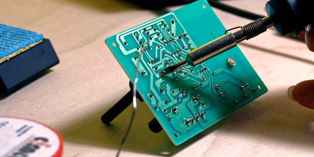
The manufacturing process for Phenolic PCBs is straightforward and does not require specialized equipment or skilled labor. This makes them ideal for small-scale production runs and for prototyping. The manufacturing process involves the following steps:
- Cut the paper to the required size and shape.
- Impregnate the paper with phenolic resin.
- Dry the impregnated paper to remove the solvent.
- Layer the impregnated paper with copper foil.
- Press the layers together under high temperature and pressure to form the final PCB.
· Good Electrical Insulation Properties
Phenolic PCBs have excellent electrical insulation properties, which makes them ideal for high-voltage applications. The phenolic resin used in these boards is an excellent insulator and can withstand high voltages without breaking down. In addition, phenolic PCBs have a low dielectric constant. It means they are excellent in high-frequency applications with low signal distortion.
· Good Dimensional Stability
Phenolic PCBs are dimensionally stable so they do not change shape or size due to temperature or humidity changes. This makes them ideal for use in harsh environmental conditions. Phenolic PCBs are also resistant to moisture, which makes them suitable for use in humid environments.
· Good Mechanical Strength
Phenolic PCBs are strong and durable, making them ideal for use in rugged environments. They are also resistant to mechanical stress, which means they can withstand vibrations and shock. This makes them suitable for use in applications such as automotive, aerospace, and industrial equipment.
Disadvantages of Phenolic PCBs
· Limited Temperature Range
One of the major disadvantages of Phenolic PCBs is their limited temperature range. They cannot withstand high temperatures and are unsuitable for use in high-temperature applications. The maximum temperature range for these boards is typically around 130°C. Above this temperature, the phenolic resin begins to break down. It can cause the PCB to become brittle and prone to cracking.

· Limited Frequency Range
Phenolic PCBs have a limited frequency range, which means they are not suitable for use in high-frequency applications. Moreover, they have poor signal integrity and are susceptible to interference. This is because the phenolic resin in these boards has a high dielectric loss factor, which causes signal attenuation.
· Poor Chemical Resistance
Phenolic PCBs are not resistant to chemicals and exposure to certain substances can damage them. This makes them unsuitable for use in applications where chemical resistance is important. Phenolic PCBs can by exposure to acids, bases, and solvents damage these PCBs. They can cause the copper foil to delaminate from the phenolic substrate.
· Poor Dimensional Accuracy
Phenolic PCBs have poor dimensional accuracy compared to other types of PCBs. This means that the size and shape of the PCB may not be consistent from board to board. This can cause problems in applications where the PCBs need to fit precisely within a specific enclosure or device. In addition, the thickness of the PCB may vary, which can affect the performance of the board.
· Limited Environmental Friendliness
Phenolic PCBs are not environmentally friendly products, as the phenolic resin in them comes from petrochemicals. In addition, the manufacturing process for these boards generates harmful waste if not properly disposed of.
Uses of Phenolic PCBs
These are popular in low-cost, low-frequency applications due to their affordability, ease of manufacturing, and good electrical insulation properties. In this section, we will discuss some of the most common uses of Phenolic PCBs.
Consumer Electronics
Engineers use phenolic PCBs in consumer electronics, such as radios, televisions, and small appliances. These devices require low-cost, low-frequency PCBs, which makes Phenolic PCBs a popular choice. They are also well-suited for small, portable devices that do not require high-performance PCBs.
Lighting
You can use phenolic PCBs in lighting applications, such as LED lights and fluorescent lamps. These applications require PCBs that can withstand high temperatures and provide good thermal management. Phenolic PCBs are able to handle the heat generated by these applications, making them an ideal choice.
Automotive
Manufacturers use phenolic PCBs in the automotive industry for applications such as instrument clusters, entertainment, and climate control systems. These applications require PCBs that are durable and can withstand harsh environments, such as extreme temperatures and vibration. Phenolic PCBs are strong and durable, making them perfect for these applications.
Industrial Control
Manufacturers use phenolic PCBs in industrial control applications, such as motor control and power supplies. These applications require PCBs that can handle high currents and voltages, and Phenolic PCBs are able to do so. They are also perfect for applications that require good electrical insulation properties.
Medical
Engineers use phenolic PCBs in medical devices, such as monitors and diagnostic equipment. These applications require PCBs that are reliable and can operate at low frequencies. Phenolic PCBs are a popular choice for these applications due to their affordability and ease of manufacturing.
Education
Phenolic PCBs are in practice in educational settings for teaching basic electronics and PCB design. They are affordable and easy to work with, making them an ideal choice for educational purposes. Phenolic PCBs can be an excellent option to teach students about basic circuit design and troubleshooting.
Manufacturing Process of Phenolic PCBs
Phenolic PCBs, also known as FR-2 PCBs, are low-cost and widely used in various industries. Understanding the manufacturing process of Phenolic PCBs can help you gain insights into their unique properties. In this section, we will take a closer look at the process of manufacturing Phenolic PCBs.
1. The Raw Materials
The first step in the manufacturing process of Phenolic PCBs is to gather the necessary raw materials. Phenolic PCBs are made up of layers of fiberglass and phenolic resin. The fiberglass provides the necessary strength, while the phenolic resin acts as a binding agent. Other materials required for the manufacturing process include copper sheets, ink, and chemicals.
2. Layering and Lamination
Once you have the raw materials, the layering and lamination process begins. Experts sandwich the layers of fiberglass and copper sheets together and coat them with a layer of phenolic resin. They place the layers into a lamination press and heated until the layers bond together. Additionally, they repeat this process several times until they achieve the desired number of layers.
3. Drilling and Etching
The next step in the manufacturing process is drilling and etching. Engineers drill the holes in the copper sheets to create the necessary connections between the layers. The engineers coat boards with a layer of ink and exposed to ultraviolet light to create a pattern. The ink is then etched away using a chemical solution, leaving behind the necessary copper traces.
4. Plating
The next step in the manufacturing process is plating. Experts coat the boards with a layer of copper using an electroplating process. This ensures that the necessary connections are strong and durable. Afterwards, they coat boards with a layer of tin or lead to protect the copper from oxidation.
5. Final Inspection
The final step in the manufacturing process is final inspection. The engineers inspect boards for any defects, such as incomplete connections or missing copper traces. Finally, they correct any defect before they ship boards to customers.
Environmental Impact of Phenolic PCBs
The manufacturing process of Phenolic PCBs involves the use of various chemicals and materials. The chemicals and materials include fiberglass, copper sheets, phenolic resin, ink, and chemicals. The disposal of these materials can have significant environmental impacts. Additionally, the disposal of Phenolic PCBs themselves can also have negative impacts, such as electronic waste and the release of toxic substances.
Recycling of Phenolic PCBs is possible. However, it is a complex and challenging process due to the nature of the materials in their manufacture. The recycling process involves separating the different materials from the PCB. These materials include copper and fiberglass and reusing them in new products. However, the presence of phenolic resin and other chemicals can make the process more difficult and expensive.
The recycling of Phenolic PCBs is becoming more common due to the increasing demand for sustainable practices. Researchers and manufacturers are exploring new ways to improve the efficiency and effectiveness of the recycling process. Furthermore, they want to reduce the environmental impact of Phenolic PCBs.
Conclusion
We have articulated everything you should know about Phenolic PCBs. This type of PCB is extremely important and has a variety of uses. If you have come across this PCB, please let us know in the comments and share your thoughts with us.
