The demand of more advanced and complex machines that can deliver what is required by the customer is increasing day by day. From military and defense sector to automation industry, consumer electronics, IoT, Medical and computer sciences, Advance research on wireless communication and microwave engineering all these sectors demand a great deal of high tech instruments, machines, equipment and devices the back bone of which is what we call “PCB”.
While we are developing our understanding in the depths of PCBs and its details, in this article we shall discuss various aspects of PCB manufacturing process, raw materials used, types of PCBs, surface finish methods, cost of manufacturing, quality, delivery time and finally tips for choosing reliable PCB manufacturer or supplier.
1- What is Printed Circuit Board manufacturing?
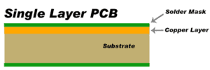
PCB is an acronym of “Printed Circuit Board”. The PCB can provide mechanical support to electronic components. It is actually a base or platform for components to reside upon and to interconnect with each other by means of copper tracks or traces. You may have noticed in many electronic products the green thick boards on to which small and large electronic components are stick on one side and on the other side the metallic sharp points of welding are seen. This green thick board is actually PCB “Printed Circuit Board” also called PWB “Printed Wiring Board”.
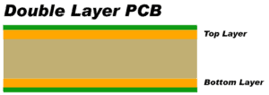
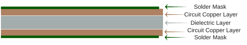
PCBs are actually divided into three categories 1- Single Sided 2- Double Sided and 3- Multilayer PCB
The single sided PCBs are those having components on top layer and connections and tracks on bottom layer. The double sided are those having components and solder pads or holes with traces/tracks on top and bottom both. Multilayer PCBs have component on top and bottom and solder pads and holes and tracks on top and bottom layers both as well as there are internal layers that contains buried and blind vias to interconnect components on top and bottom. The vias are the small opening in PCBs that is used to connect the top and bottom and inner layers with each other. The blind via is the one that has one end at either on top or bottom and other end is somewhere inside the inner layers. The buried via is the one having both ends “buried” inside the inner layer. The solder pads are made of solder paste on PCBs onto which SMT components are soldered. The plated through holes made by boring or drilling in the mass produce pcb are used to mount THT components
2- Different Layer PCB Manufacturing Process
A. Single Layer PCB manufacturing Process:
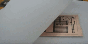
This process is not for mass manufacture but for single prototype development of single layer PCB for hobbyists. All materials used here is easily available and this PCB can be made in home easily
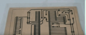
Step-1: Design the PCB layout from the schematics on any CAD EDA tool like Altium. Then create Gerber files and print your layout on the OHP sheet using laser printer.
Step-2: The fiber glass FR4 substrate base material is used. The copper clad is laminated on one side after soaking in epoxy resin.
Step-3: Rub the copper side of FR-4 with steel wool to remove oxide and photo resists if any.
Step-4: Place the OHP sheet on top of the copper side of FR-4
Step-5: Place the white paper on top of the OHP sheet and press with iron. The heat will cause the ink to stick to the copper plate exactly as it is on OHP
Step-6: Allow the PCB to cool and slowly remove OHP sheet.
Step-7: Now make a solution of Ferric Chloride and dip the PCB in the solution for 30 minutes. This solution will eat away the copper that is exposed to ink. Hence leaving the copper that is under the ink. This is called etching of unwanted copper.
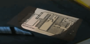
Step-8: Remove the PCB and wash with cold water and rub with steel wool to clear the ink the resulting conductive copper tracks are created as per circuit diagram.
Step-9: Carefully drill on pads
Step-10: Put the components in drill holes and solder them
B. Double Layer PCB manufacturing Process:
Step-1: The PCB layout design is made in CAD software and Gerber generated for top and bottom layers both. These images are printed on photographic film (transparencies or OHP) by means of photo plotter.
Step-2: The copper clad on both sides of FR-4 substrate base material is chosen. The sheet is cut in an appropriate size so as to accommodate as many as individual boards on single sheet as possible. This sheet is the PCB “Panel”. In this we can reduce manufacturing cost.
Step-3: The two separate photo films (negative) are created for top and bottom. The black ink is used to prevent the UV rays passing and hence makes the copper trace and pads.
Step-4: The photo resist film is placed on the entire substrate board. After that, the top film is placed upon the photo resist film.
Step-5: The stack of copper clad FR-4 substrate, photo resist and photo film is then exposed to Ultra Violet (UV) radiation. The black ink will protect the UV rays to penetrate through the resist and thus this resist beneath will be washed off.
Step-6: The photo resist that is exposed directly to UV will harden (polymerize) hence creating pads and tracks.
Step-7: The steps 4-6 are repeated for bottom layer also
Step-8: Next the solution of ferric chloride is prepared and the PCB is dipped to etch away unwanted copper from top and bottom side that is not beneath the photo resist.
Step-9: After unwanted copper is etched away, the wanted copper under the photo resist is protected and not etched away. Now photo resist is removed using another chemical solution
Step-10: Now the PCB with exposed copper tracks and pads is ready. It is time to drill holes and vias as per the drill file generated with extended Gerber. Via is used to connect the top and bottom layers components pads.
Step-11: The registration holes are bored to secure the board in place so it will not move to protect missed drill hits or misalignment of holes. Now the automated machine that is fed drill guide with extended Gerber files will automatically bore holes in PCB.
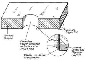
Step-12: Electro less Plating copper is now done using chemical deposition. The PCB undergoes chemical baths and surface of panel gets 1 micron thick copper. This copper is then deposited upon the walls of drills bored in the previous step. Next the panel plating is done.
Step-13: Solder mask epoxy ink is applied. There are various colors available green, blue and red. Green is widely used. The PCB is moved to oven to secure the solder mask appropriately.
Step-14: Surface Finish is done ENIG, HASL (Hot Air Solder Leveling)
Step-15: Final electrical testing
C. Multilayer Layer PCB manufacturing Process:
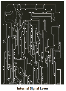
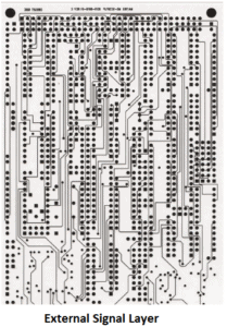
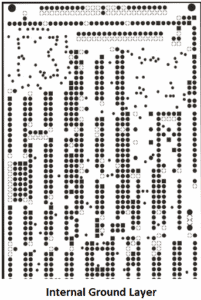
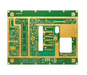
The multilayer PCBs are those having layers of copper more than 2. The manufacturing process / fabrication of multilayer PCBs is relatively more complex than single and double sided PCBs. This is because of additional layers of ground or power plane and additional signal layers inside the PCB board. The multilayer PCBs are thicker, heavier and dense containing hundreds of SMT and THT components populated upon top and bottom surfaces to achieve more electronic functions from PCB. resin plug hole hdi pcb is the example of multilayer PCB. The multilayer PCB can go up-to 30 layers stack to perform more advance electronic functions including digital, analog and hybrid circuits. There are some multilayer PCBs that have reached 100 layers limit but the cost of pcb manufacturing and assembly is very high and fabrication process is also very complex.
Below is the step by step procedure of a general multilayer PCB up-to 4-6 layers.
Step-1: Initial Setup at PCB Fab Shop:
The electronics engineer or any competent design will design the circuit and layout the PCB in suitable CAD (EDA) software/tool like EAGLE or ALTIUM. The Gerber files, drill files, pick and place files along with other necessary layout files are generated. This fabrication data is sent to the PCB fabrication shop. The staff at PCB fabrication shop will analyze this data, perform data cleanup, drill and rout data verification, perform PCB edits and penalization. Lastly, final output files are generated.
Data Cleanup: It means to check the layer alignments and file names or assignments/designators in the software available at PCB fabrication shop. The different software or tool will generate different results in Gerber and ODB++ files hence data cleanup and alignment is necessary
Drill and Rout Drawings Verification: Drill size, drill count, plated and non-plated holes are verified against the fabrication drawing provided by designer. Unusual routing and cutout is also checked that may require separate file for each process.
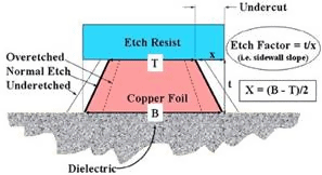
Run DRC and DFM: The CAM engineer at PCB fabrication shop will then run the DRC (Design Ruler Check) and DFM (Design for Manufacturing) checks to edit any errors pertaining to solder mask, silk screen, copper layer, drill sizes, minimum clearance issues and to add etch compensation. Etch compensation is the ratio of depth of etch to the amount of lateral etch. In other words “The ratio of conductor thickness to undercut”. See diagram.
Making PCB Panels: The PCB panel is cut in such a way to ensure limited waste of material, best fit for maximum individual boards and best pricing to achieve maximum profitability in mass manufacturing.
Outputs Files: Finally all data files, Gerber, drill, rout, and image and AOI files are generated. These files are fed to automated computer controlled machines being operated remotely by competent engineer.
Step-2: Choosing the Material:
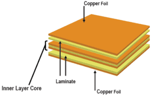
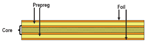
The core base substrate laminate of FR-4 fiber glass material is chosen. The thickness of core can be from 0.038” to 0.005” depending upon the application/usage of bare PCB. There can be multiple cores in one single PCB board also depends on design and application. The FR-4 laminated copper clad panel is selected in standard size of 18 x 24 square inch.
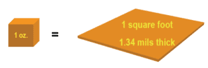
The ½ and 1 ounce (oz) per square foot of copper in weight is used or 0.0007 to 0.00134 inch thick copper foils can be used. The measurement of copper thickness is done in “ounce” for PCBs. For instance a PCB (size = 1 square foot) that uses 1 oz of copper has a copper thickness of 1.34 mils.
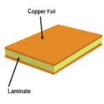
The PCB panel stack is made up of core, copper foil, and prepreg. The pre-preg is the bonding glue that binds the cores together. Commonly the FR-4 is pre-impregnated with “epoxy resin”. This epoxy resin glue layer is melted upon heat and pressure during “lamination” stage thus cooling and bonding layers and cores together.
Note: There are latest advance machine like LDI “Laser Direct Imaging” method used to plot images directly on dry film resist without using OHP sheet. This is done for all inner layers and outer layers as well. This method reduce cost and speeds up the process with high accuracy.
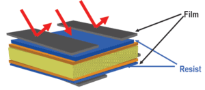
Step-3: Apply Photo Resist:
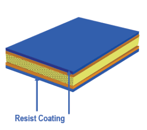
Now as seen from the figure the FR-4 laminate is sandwiched between the copper foil. Now the stack’s top and bottom will be covered with dry-film photo resist in blue color by applying heat and pressure as shown in figure below. This photo resist film is sensitive to Ultra Violet (UV) Radiation. Yellow color light is used in dark rooms of PCB fabrication shop to polymerize the photo resist sheet.
Step-4: Make Photo Tools and Art-Work:
Now that all the files are ready, we now have to photo plot these images onto the piece of transparent film called OHP sheet. The machine used to plot these PCB images for each individual layer is called photo plotter. The PCB images including drills, pads, traces, metal grounds, solder masks, legends, nomenclature and any other copper feature are plotted on the OHP sheet.
Each layer has separate image and printed separately on separate OHP sheet.
The inner film layer is negative and outer/external film layer is positive. Each film layer has unique pattern of art work. The black ink will block the UV light to hit the photo resist while the clear/transparent area will “through” the UV radiation. The photo resist pattern where UV light falls will harden/polymerize and the copper beneath will become traces/tracks/pads. The unwanted copper on top of which the photo resist is “not harden” will be etched away chemically in later steps.
Negative film means the copper patterns are formed on the areas that are transparent. Positive film means the copper pattern are formed on the areas that are opaque.
Step-5: Exposure to UV:
Now the panel stack is exposed to high intensity UV radiation. The radiation passes through the negative film for inner layers and positive film for outer layer. Each layer one by one is exposed to UV through corresponding films and circuit pattern is printed on photo resist by UV that passes the transparent regions of film. Thus hardening the photo resist.
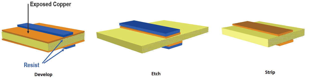
Step-6: Develop Etch Strip (DES):
Develop: The chemical solution or developer is used to remove the photo resist that was not polymerized/hardened.
Etch: Now the copper is etched away from all those sections that were not covered by dry film photo resist by means of chemical solution like ferric chloride. The photo resist and copper pattern become same and FR-4 substrate will emerge as copper is etched away.
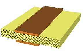
Strip: The photo resist on top of the copper traces is now removed chemically. Thus leaving the copper traces, pads, ground plane and other copper features.
Step-7: Automated Optical Inspection (AOI):
Next step is to run the AOI check. The inner layers are inspected one by one for any defect regarding open “missing copper” or shorts “excess copper” by comparing them with actual image in Gerber files and design data. This is done before lamination process. At this stage any possible defects can be detected and removed. At later stage after lamination it will be impossible and too late to undo or discover any possible defect hence AOI is critical step to find any flaws in the inner layers at this stage.
Step-8: Oxide Coating:
The oxide layer coating is the chemical treatment of applying black or brown oxide on inner layers to increase adhesive power and roughness of copper clad and augment laminate bond strength. This helps tighter lamination of inner layers and prevents delamination in manufacturing process.
Step-9: Lamination:
The hydraulic press is used to apply high pressure and heat to the stack of core, inner layers, pre-preg and outer copper foil layer. The pre-preg will melt as a result thus joining the layers together. The stack will cool and strengthens the bond between core and layers.
Step-10: Drilling:
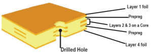
The most important part in PCB fabrication is drilling the holes. The NC Drill File is the necessary files which the beginner designers forget to submit to the fabrication shop. These NC (Numeric Controlled) Drill files have the digital data that is fed to the CNC (Computer Numeric Controlled) drilling machines that are advance and contains solid carbide drilling bits, which in turn drill the bores / holes according to the size and location. The drilling machine automatically picks and replaces the appropriate drill bit according to the size of drill hole. The hard cardboard is placed at the exit location of drill bit, so as to avoid burr in copper foil.
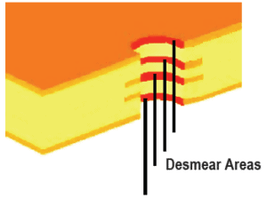
De-burr: This is the mechanical process of buffing, polishing and trimming the raised edges around the holes that occurred during drilling process.
De-Smear: This is the process of removing the thin coating of resin from inner layers that is created by heat and motion of drilling bits. Removing the resin smear can increase electrical conductivity.
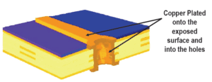
Step-11: Electro-less Copper Plating:
This is the chemical deposition of copper on to the hole walls and exposed surface of panel. A very thin conductive layer of copper is deposited on the fiber glass walls of holes drilled in previous step. The thickness of electro-less plated copper is inch.
Step-12: Dry Film Outer Layer:
Same as done for the inner layers, the outer layer is coated with dry film photo resist again. The whole panel including the drilled holes is completed covered with photo resist.
Step-13: Outer Layer Expose and Develop:
In this step the panel is exposed to UV radiation same as done for inner layers. The UV radiation will pass through and hardens the dry film photo resist thus creating an image of circuit pattern. The drilled holes are also exposed and electroplated in next step.
Step-14: Electroplating:
The PCB panel is now electroplated in copper plating bath (an electrolyte of copper sulfate) to apply current to anode and cathode bars by means of DC power supply. When the current is applied, the copper from the bath is deposited on the conductive surface of panel and on the hole walls. The thickness of copper deposited is 1 mil.
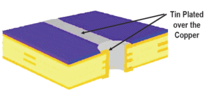
Step-15: Tin Plating on Outer Layer:
The tin plating is required on all exposed copper to resist the etching away of copper during etching of photo resist from top layer and to maintain the copper traces, pads and other copper features on outer layer.
Step-16: Resist Striping on Outer Layer:
The developed (that resist that was not exposed to UV) dry film photo resist is etched away. The copper under the tin plating is not affected. The holes under the resist will uncover and will be non-plated.
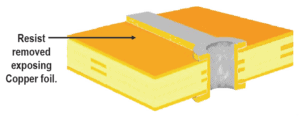
Step-17: Copper Etching on Outer Layer:
Copper is now once again removed from outer layer from all those areas where which were not covered by tin. Tin again resist the etching away of copper underneath it and traces, pads and other art work is left behind on panel.
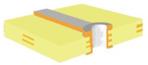
Step-18: Tin Stripping from outer Layer:
Now the tin is stripped off the outer layer done by chemical solution. Leaving behind exposed and bare copper trace, pads and other copper features.
Step-19: Cleaning:
Now the final PCB panel with exposed copper traces, pads, PTH (Plated through Hole) and other copper features are cleaned thoroughly, and ensure oxidation free before going to apply solder mask in next step. Pumice is used to scrub the panel surface to ensure contamination free surface and ensure adhesion of solder mask.
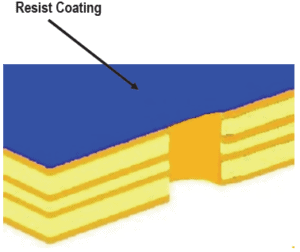
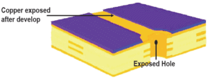
Step-20: Solder Mask Application:
In this step now the solder mask is applied. It is Liquid Photo Image-able mask that is available in green, red or blue colors. However green color solder mask is common. The technique of Photolithography (same as used in imaging the copper traces in previous steps) is used in which panel is exposed to UV radiation through a film tool. All the exposed solder mask will remain and unexposed solder mask will be removed through the “developer” processing. After this the remaining solder mask is “cured” by baking the panel in oven. The main purposes of solder mask is to give color to the PCB, protect panel from contamination, accidental shorting during mishandling,
Step-21: Silk-screening
The names, nomenclature, component designators, Logos and part numbers with date and company name can be printed on PCB panel by screen-printing. The color of ink usedis white. The panels are baked again to cure ink.
Step-22: Surface Finish:
The surface finish step is conducted by Hot Air Solder Leveling (HASL). The whole panel is applied with flux (a viscous material that aids soldering) then the panel is dipped into the tub of molten solder. The molten solder will stick to the exposed metal surface. When the panel is removed, high pressure hot air is blasted on the surface of panel that will remove excess solder from holes and evens the surface pads.
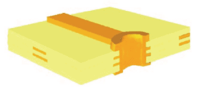
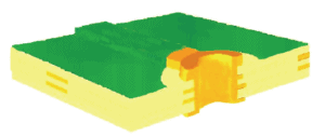
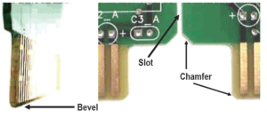
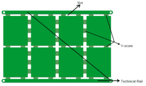
Step-23: Routing, Scoring, Bevel:
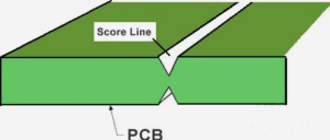
It is now time to cut out the individual boards from PCB panel. This is done by “routing” the “scoring lines” so they can be broken off easily. This is done by cutting the V-shaped groove on top and bottom of PCB panel around the borders of individual board. This is also known as V-Groove scoring or V-Scoring. The chamfer, bevel and slots are added after this. See the figure.
Step-24: Electrical Testing:
Now the individual boards are electrically tested, by flying probe test. The board is given electrical signals according to the netlist or test program provided by designer and shorts and opens are identified if any. There are many test points on the board so electrical testing can be a lengthy process. On the basis of test results the board is either repaired or discarded.
Step-25: Final Inspection:
The board is finally visual inspected and verified for customer requirements
Step-26: Packaging and Delivery:
The boards are then properly packed and wrapped in vacuum protective packaging or ESD protective packing if required and ready to ship.
Common Terminologies to Remember:
- Annular Ring: The ring around the PTH in a PCB
- Drill hit: is the place on the PCB where the hole is to be drilled.
- Gold Finger: These are the exposed pads on PCB that intends to insert that PCB in another PCB with socket. Example RAM and mother board.
- Mouse Bites: These are the alternative to V-Groove cut to separate the PCB from panel
- Thermal Pad: This is the pad used in PCB layout to enable the heat transfer during soldering and de-soldering of component. The thermal pad should be properly relieved.
3. PCB raw material For Manufacturing:
There are numerous materials available for PCB manufacturing. Some of them are
A. FR-4 PCB Manufacturing:
The most common and widely used PCB base material is FR-4. The FR-4 (stands for Fire Retardant FR-4) is good insulator with significant mechanical strength, available in pre-impregnated with epoxy resin made of fiber glass substrate laminate. The copper clad FR-4 material are easily available at low cost and have high durability, low water absorption and self-extinguishing flammability properties.
B. Metal Core PCBs:
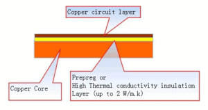
The metal core PCBs (MCPCBs) are the vital solution to high power electronic devices like LEDs. The lighting white color LEDs are nowadays very commonly used in houses, offices, streets and many other places. These ultra-thin lcd pcb are driven by electronic circuits like ballast or other high current drive circuits. These circuits are made up of MCPCBs. These copper-aluminum composite pcb are made of metallic core like copper or aluminum (specifically formulated) in order to draw heat thermally (due to high thermal conductivity of dielectric) from hot-running component like LED through metallic core towards the back layer where it dissipates efficiently in heat sink. These MCPCBs are very useful in devices that tend to dissipate more heat and consume lots of power.
1- Copper MCPCBs:
There are three main metals copper, aluminum and steel alloy to use as metal cores. Copper has best performance for thermal conductivity than aluminum and steel both but the cost is high. While copper cannot provide such mechanical strength as steel alloy.
2- Aluminum MCPCBs:
The aluminum is mostly preferred metal for copper-aluminum composite pcb. This is widely used in LED lights where 100s of watts is dissipated efficiently. While aluminum is not much expensive and also provide moderate mechanical strength to PCB overall with good thermal conductivity.
3- Steel Alloy PCB:
Steel alloy MCPCBs are cheap but thermal conductivity is not too good as compared to copper and aluminum. While they provide good mechanical strength to specialize pcb.
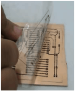
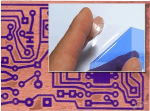
C. Flexible PCB:
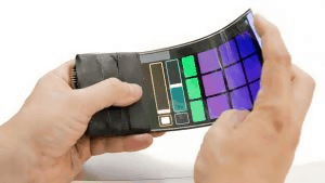
The substrate material of Flex PCBs is plastic, Polyether ether Ketone (PEEK) and Polyimide (Pi). The flex PCBs are not rigid and can be “bend” or twisted as required. They are high in demand in electronic equipment where space constraint is the main issue. The flex PCB cables are widely used in many electronic devices like cameras, automobile electronics and instruments panels. The latest technology of OLED has been upgraded to Flex PCBs (FOLEDs)
D. High Frequency PCBs:
Telecommunication devices are made up of special kind of PCBs that can carry high speed high frequency signals in the routes/traces without disrupting the signal and with good noise immunity and with least interference. This cannot be possible without using special types of PCB substrate material that facilitates high frequency signal transmission. These materials are Rogers, Taconic, Arlon, Teflon, Nelco, Isola and FR-5.
1- Rogers PCB:
Rogers Corporation is actually a company that produces laminates for RF PCBs. Rogers (RO3003) is ceramic filled PTFE composite, widely used laminates in commercial RF devices. Dielectric constant (DK) in the range of 3.0 to 10.2. Low TCDK for electrical stability vs temperature. Low Z-Axis Coefficient of Thermal Expansion (CTE) 24 ppm/C gives reliable PTH. Widely used in cellular devices, RFID tags and satellite communication devices and antennae from 500 MHz to 10GHz.
2- Taconic PCB:
Taconic is also a company that produces ceramic filled PTFE laminates for RF/Microwave PCBs. RF-35 is the suitable material for high volume production of commercial RF devices. That is low cost material, low absorption of moist and low dissipation factor (DF = 0.0018). Dielectric constant DK is 3.5 +/- 0.1.
3- Arlon PCB:
Arlon is yet another RF PCB substrate manufacturing company, that specializes in high Tg, low loss thermoset laminate and multifunctional epoxy. The 33N is a flame retardant polyimide laminate and prepreg system where Junction Temperature (Tg) can go up-to 350OC. Arlon specializes in military applications and avionics aircraft engine instrumentation PCBs. Dielectric constant at 1 MHz is 4.25 while dissipation factor is 0.01 @ 1 MHz Decomposition temperature Td is 389 @ 5%.
4- Teflon PCB:

Teflon is another name of PTFE. So all those PCBs discussed above containing PTFE falls in the category of Teflon PCB. The PTFE stiffness is improved by adding large number of SiO2 or fiber glass as filling material. Teflon is highly expensive and is used as base substrate material in Microwave PCBs requiring operational frequency greater than 10 GHz. It has very low Dk and DF values and highly heat resistant.
5- Nelco PCB:
Yet another PCB laminate and Prepreg manufacturer is Nelco. The Meteor-wave 1000NF is a resin system that is used in very high speed PCBs, low loss digital electronic circuits. This is the material offering very advance electrical performance and high reliability. This is the prepreg designed for bonding flex circuitry and heat sinks to rigid circuits. Suitable for high temperature lead free assemblies and high layer count RF PCBs. Dielectric constant Dk = 3.4 and DF = 0.0047 @ 10 GHz. Tg = 240OC.
6- Isola PCB:
Isola specializes in high speed digital circuits and high density interconnect (HDI) PCBs. The IS680 AG-348 is a very low loss laminate material. The ultralow dissipation factor DF = 0.0029 @ 10 GHz. The dielectric constant is Dk = 3.48 @ 10 GHz. Decomposition Temperature Td = 360OC and Junction Temperature Tg = 200OC
7- FR-5 PCB:
FR5 Laminate is a glass fabric reinforcement in a high temperature epoxy resin binder. This has superior mechanical properties and higher operating temperature. The junction temperature Tg ranges from 170 to 180OC. Continuous operating temperature is 140 degree C. Highly suitable for multilayer PCBs with high layer count. Applications in automotive, aerospace, electrical equipment and antennal isolators.
E. Surface Processing of PCB Manufacturing:
HASL and lead-free HASL
Lead free HASL is a low cost option for surface finish of PCB, but with rising trend of SMT technology and fine pitch components, the use of HASL does not make sense because it leaves uneven surfaces. It is not good for fine pitch plated through hole and has poor wetting.
OSP (Organic Solder-ability Preservative)
OSP is an organic surface finish method that is water based. It is typically used for copper pads. It is lead free, good for flat surfaces, process of applying OSP is simple while having short shelf life and sensitive handling and not good for PTH.
Highly suitable for planar surface fine pitch components and commonly used with back planes. It protects underlying copper from oxidation. The metallic nature can create problem when merged with copper to reduce shelf life and performance of surface finish. It is cost effective, reliable, suitable for reflow solder but not suitable for PTH, handling dangers, tin wiskering and can damage solder-mask.
This is the most suitable process of surface finish that outweighs its cost as compared to its benefits. Appropriate alternative to ENIG, useful for fine pitch and flat pack coating. Uniformity in finish and moderate shelf life of 12 months. It contains OSP that prevents ruining/oxidation. The PCBs surface finished with immersion silver should be packed immediately because immersion silver is contaminant sensitive. Used in aluminum wire bonding and membrane switches and EMI shielding.
Electro-less Nickel Immersion Gold (ENIG):
ENIG is expensive and suitable for complex surface mount components like BGA and Flip Chips based PCBs. It is a double layer coating of metal. Nickel acts as barrier between surface on which components are soldered and copper. A gold layer protects nickel during storage. The gold along with nickel can build phosphorus layer that can result in fractured surface and faulty connections. It is good for PTH, lead free, strong and suitable for flat surfaces.
F. PCB Manufacturing Capability:
1- Rigid PCB Capacity:
At Rayming PCB, we have the capacity of manufacturing rigid PCBs up-to 36 layers, maximum board thickness 8.5mm, minimum board thickness for 6 layers is 0.6mm, minimum layer clearance 0.1mm, min line width 0.075mm, minimum line space is 0.075mm and minimum hole size is 0.15mm. More constraints and capacity can be found here.
2- Metal Core PCB Capacity:
At Rayming PCB, we have the capacity of manufacturing metal core PCBs up-to 2 layers, base material is aluminum and copper, thickness is 0.02 to 0.18 inch, surface treatment available is Lead Free HASL, ENIG, OSP. More information can be found here.
3- Flexible PCB Capacity:
At Rayming PCB, we have the capacity of manufacturing flex PCBs up-to 1-6 layers, material used PI, PET, PEN and FR-4, thickness 0.002” to 0.1”, surface finish ENIG, OPS, immersion silver, immersion tin, minimum board size is 0.2”x0.3” and maximum board size is 20.5”x13”. For more information please click here.
4- Rigid Flex PCB Capacity:
At Rayming PCB, we have the capacity of manufacturing rigid flex PCB up-to 2-8 layers, board thickness 0.0024” to 0.16”. More information click here.
G. PCB Manufacturing Cost
The main factors that determine the PCB manufacturing cost are
- Panel Size: The bigger the panel size the higher the initial cost
- Lead Time: Shorter lead time higher cost and vice versa
- Layers: Multilayer PCBs are costly because they require additional raw materials and complex manufacturing process while single and double sided layers are not expensive.
- Inspection: The final inspection and electrical testing in PCB fabrication process adds up more cost to the overall PCB manufacturing process
- Surface Finish: Choose the surface finish that appropriately fulfills your requirements. Selecting the right surface finish method can adjust your PCB manufacturing cost effectively.
- Drill count and Drill Size: The more the drill count and more the variation in drill sizes the higher the cost of PCB manufacturing and vice versa.
- Vias: The more the vias the more complex the PCB and higher cost.
H. Quality Guarantee of PCB Manufacturing:
The quality of PCB manufacturing is dependent of the manufacturing process itself and the selection of raw materials for PCB. As per the application and requirements the PCB raw material is chosen, for RF PCB the ceramic PTFE base is selected while for commercial low frequency PCBs FR-4 is good reasonable to ensure good quality PCB. Also the surface finish method and inspection also plays important role in high quality PCBs.
I. PCB Manufacturing Deliver Time:
It is vital to understand that short delivery time adds to cost of PCB manufacturing. Thus for smaller consignments or orders it is recommended to use express freight. For medium scale PCB orders use air freight and for larger PCB orders use Sea Freight. In some countries like Pakistan, the custom clearance charges are to be paid by the customer and not by the PCB manufacturing company. Thus it is important to know your country’s customs rules and regulations to avoid any delays and unnecessary go down charges that may apply.
J. Tips for Choosing PCB Manufacturing Supplier:
On-Time Delivery: It is important to do some initial research about various suppliers online available. Check their time line for order delivery. Check the method of freight they offer and any refund policies they have.
Reputation: A good reputation PCB manufacturer or supplier is always reliable. A supplier having 5 star ratings must be your top priority. Read feedback and comments of other customer to get initial know how. Check the profile of company to know about its services and products
Customization: A supplier that is open to customized PCB design and manufacturing is a good option.
Latest Technology: A PCB manufacturer using latest technology, latest equipment for PCB manufacturing and latest CAD software for handling data files must be your option
All under one roof: It is important that you select a PCB manufacturer that provides all services from PCB design to final PCB product including PCB assembly. This will reduce your hassle to deal with different PCB manufacturers and assemblers at the same time.
