Power supply layout design is a crucial aspect of electronic circuit design. It involves the arrangement of components on a printed circuit board (PCB) to ensure efficient and reliable power delivery to the circuit. Poor power supply layout design can lead to various issues, including noise, voltage drops, and electromagnetic interference (EMI).
One of the primary goals of power supply layout design is to minimize the length and impedance of the power and ground traces. These traces should be as short as possible to reduce resistance and inductance, which can cause voltage drops and noise. Additionally, proper placement of decoupling capacitors near the power and ground pins of integrated circuits (ICs) can help to filter out noise and ensure stable power delivery.
Overall, effective power supply layout design requires careful consideration of the placement and routing of power and ground traces, as well as the use of decoupling capacitors and other filtering components. By following best practices and guidelines for power supply layout design, engineers can ensure optimal performance and reliability of their electronic circuits.
Key Considerations
When designing a power supply layout, there are several key considerations that must be taken into account to ensure optimal performance. These include component selection, thermal management, noise reduction, and electromagnetic interference (EMI).
Component Selection
The components used in a power supply layout can greatly impact its efficiency and reliability. When selecting components, it is important to consider factors such as voltage rating, current rating, and temperature rating. Choosing components with higher ratings than necessary can result in unnecessary cost, while choosing components with lower ratings can lead to premature failure.
Thermal Management
Heat is a common issue in power supply layouts, and proper thermal management is essential for maintaining optimal performance and preventing damage to components. This can be achieved through the use of heat sinks, thermal pads, and other cooling mechanisms. It is also important to consider the placement of components to ensure adequate airflow and minimize heat buildup.
Noise Reduction
Noise can be a significant issue in power supply layouts, as it can interfere with the performance of other components and systems. To reduce noise, it is important to use high-quality components and minimize the length and impedance of signal paths. Shielding and filtering can also be used to reduce noise.
Electromagnetic Interference (EMI)
EMI can be a major issue in power supply layouts, as it can cause interference with other components and systems. To minimize EMI, it is important to use proper grounding and shielding techniques. The layout should also be designed to minimize the length and impedance of signal paths, and components should be placed to minimize the coupling of electromagnetic fields.
In conclusion, when designing a power supply layout, it is important to carefully consider component selection, thermal management, noise reduction, and EMI. By taking these factors into account, you can ensure optimal performance and reliability of your power supply.
Layout Techniques

Grounding and Power Planes
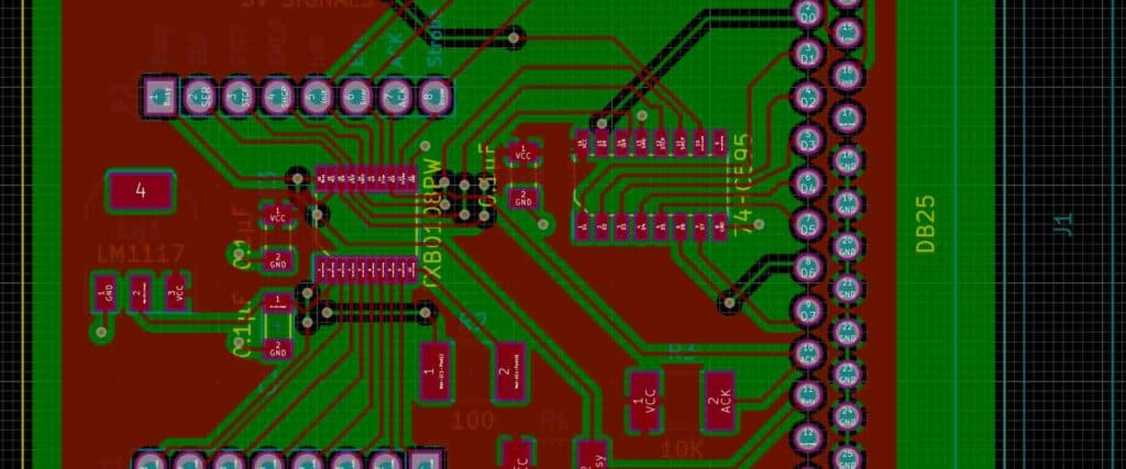
One of the most important aspects of power supply layout design is the grounding and power planes. The ground plane should be as large as possible and should be connected to all the components that require a ground connection. The power plane should be designed to provide adequate power to all the components in the circuit. The power and ground planes should be placed as close to each other as possible to minimize the loop area and reduce the inductance.
Decoupling Capacitors
Decoupling capacitors are important components in power supply layout design. They help to filter out noise and provide a stable voltage to the components. It is recommended to place decoupling capacitors as close to the power and ground pins of the components as possible. A good rule of thumb is to place one decoupling capacitor for every two to three components.
Traces and Routing
Traces and routing are also important aspects of power supply layout design. It is recommended to use wide traces to reduce the resistance and inductance of the circuit. The traces should be routed in a way that minimizes the loop area and reduces the inductance. It is also important to avoid routing high-speed signals near the power and ground planes to reduce noise.
Signal Integrity
Signal integrity is critical in power supply layout design. It is important to ensure that the signals are not distorted or degraded as they travel through the circuit. This can be achieved by using proper termination techniques, avoiding long traces, and minimizing the loop area. It is also important to avoid routing high-speed signals near the power and ground planes to reduce noise.
In summary, power supply layout design is a critical aspect of circuit design. Proper grounding and power planes, decoupling capacitors, traces and routing, and signal integrity are all important considerations. By following these techniques, you can ensure that your circuit operates reliably and efficiently.
Testing and Validation
When it comes to power supply layout design, testing and validation are critical steps to ensure the design meets the requirements and specifications. The testing process should include power integrity analysis, signal integrity analysis, and thermal analysis.
Power Integrity Analysis
Power integrity analysis is the process of verifying that the power delivery network (PDN) is capable of delivering clean, stable power to the components on the board. This analysis involves measuring the voltage and current waveforms at various points on the board and comparing them to the target specifications. The following methods can be used for power integrity analysis:
- DC voltage drop analysis
- AC impedance analysis
- Transient analysis
Signal Integrity Analysis
Signal integrity analysis is the process of verifying that the signals on the board are free from noise and distortion. This analysis involves measuring the signal waveforms at various points on the board and comparing them to the target specifications. The following methods can be used for signal integrity analysis:
- Eye diagram analysis
- Time-domain reflectometry (TDR)
- Frequency-domain reflectometry (FDR)
Thermal Analysis
Thermal analysis is the process of verifying that the temperature of the components on the board is within the safe operating range. This analysis involves measuring the temperature at various points on the board and comparing them to the target specifications. The following methods can be used for thermal analysis:
- Steady-state thermal analysis
- Transient thermal analysis
- Worst-case thermal analysis
In conclusion, testing and validation are critical steps in power supply layout design. Power integrity analysis, signal integrity analysis, and thermal analysis are the key methods used in the testing process. By following these steps, designers can ensure that their designs meet the requirements and specifications.
Conclusion
In conclusion, power supply layout design is a crucial aspect of any electronic circuit design. A well-designed power supply layout can significantly improve the performance and reliability of the circuit. On the other hand, a poorly designed power supply layout can lead to a range of issues, including noise, voltage drops, and instability.
To achieve a good power supply layout, it is essential to follow some fundamental design principles. These include minimizing the length of the power traces, using proper decoupling capacitors, and separating analog and digital circuits. Additionally, using a ground plane can help reduce noise and improve signal integrity.
It is also important to consider the thermal management of the power supply. Adequate heat dissipation can prevent overheating and ensure the longevity of the components.
Overall, a good power supply layout design requires careful planning, attention to detail, and an understanding of the circuit’s requirements. By following these principles and guidelines, designers can ensure that their circuits operate reliably and efficiently.
