PT2399 is a popular integrated circuit that is widely used in the audio industry. It is a digital echo processor that can produce a range of sound effects, including delay, reverb, and chorus. One of the critical factors that determine the performance of this IC is the PCB layout.
The PT2399 PCB layout plays a crucial role in the overall performance of the circuit. A well-designed layout can minimize noise and interference, reduce signal loss, and improve the overall sound quality. On the other hand, a poorly designed layout can result in a range of issues, including distortion, noise, and signal loss.
Designing a PT2399 PCB layout requires a thorough understanding of the circuit’s requirements, the characteristics of the components used, and the principles of good PCB design. It involves careful placement of components, routing of traces, and proper grounding techniques. With the right design, the PT2399 can produce high-quality sound effects that are widely used in the audio industry.

PT2399 PCB Layout Design Considerations
Schematic Design
The schematic design for a PT2399 PCB layout should include the basic components that are required for the PT2399 to function properly. These components include resistors, capacitors, and the PT2399 IC itself. The schematic should be designed in a way that allows for easy routing of the PCB.
Component Placement
When placing components on the PCB, it is important to consider the physical layout of the board. The placement of components can affect the overall performance of the circuit. For example, placing the PT2399 IC too close to other components can cause interference and noise. It is also important to place the components in a way that allows for easy routing of the PCB.
Routing Guidelines
Routing the PCB is an important part of the design process. The routing should be done in a way that minimizes noise and interference. The routing should also be done in a way that allows for easy testing and troubleshooting. It is important to keep the traces as short as possible to reduce noise and interference.
Grounding Techniques
Grounding is an important aspect of PCB layout design. Proper grounding can help reduce noise and interference. It is important to have a solid ground plane and to keep the ground traces as short as possible. It is also important to separate the digital and analog grounds to reduce noise.
In summary, when designing a PT2399 PCB layout, it is important to consider the schematic design, component placement, routing guidelines, and grounding techniques. By following these guidelines, you can create a PCB layout that is optimized for the best performance of the PT2399 circuit.
PT2399 PCB Layout Best Practices

Power Supply Design
The PT2399 requires a stable and clean power supply to function properly. Therefore, it is crucial to design a power supply that meets the requirements of the PT2399. The power supply should be regulated and filtered to minimize noise and ripple. A decoupling capacitor should also be placed close to the power pins of the PT2399.
Clock Circuit Design
The clock circuit is an essential part of the PT2399 circuit. It generates the clock signal that controls the delay time of the PT2399. A stable and accurate clock signal is crucial for the proper functioning of the PT2399. Therefore, it is recommended to use a crystal oscillator or a high-quality clock generator to generate the clock signal.
Signal Integrity Considerations
Signal integrity is critical in any audio circuit, and the PT2399 circuit is no exception. To ensure good signal integrity, it is recommended to keep the signal traces short and avoid running them parallel to noisy traces. The signal traces should also be shielded from noise sources, such as power and ground traces.
Noise Reduction Techniques
Noise is a common problem in audio circuits, and the PT2399 circuit is no exception. To reduce noise, it is recommended to use a ground plane and keep the signal traces away from noisy traces. It is also recommended to use bypass capacitors to filter out high-frequency noise. Finally, it is important to keep the input and output traces separated to avoid crosstalk.
In summary, designing a PCB layout for the PT2399 requires careful consideration of the power supply, clock circuit, signal integrity, and noise reduction techniques. By following these best practices, you can ensure that your PT2399 circuit functions properly and produces high-quality audio.
PT2399 PCB Layout Examples
When designing a PT2399 PCB layout, there are two common approaches: single-sided and double-sided. Both have their advantages and disadvantages, and the choice often depends on the specific project requirements and constraints.
Single-Sided Layout Example
Single-sided PCB layouts are simpler and cheaper to manufacture, making them a popular choice for hobbyists and small-scale projects. However, they are also more limited in terms of routing options and component placement.
A typical single-sided PT2399 PCB layout might look something like this:
In this example, the PT2399 chip is located in the center of the board, with the input and output jacks on either side. The potentiometers and bypass switch are located at the bottom of the board, and the power supply components are located at the top.
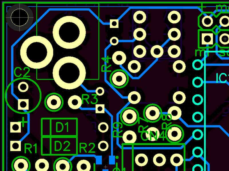
Double-Sided Layout Example
Double-sided PCB layouts offer more flexibility and routing options, making them a better choice for more complex projects. However, they are also more expensive to manufacture and require more careful planning and design.
A typical double-sided PT2399 PCB layout might look something like this:

In this example, the PT2399 chip is located in the center of the board, with the input and output jacks on the left and right sides, respectively. The potentiometers and bypass switch are located at the top of the board, and the power supply components are located at the bottom.
Overall, the choice between single-sided and double-sided PCB layouts depends on the specific project requirements and constraints. Both approaches have their advantages and disadvantages, and it is up to the designer to choose the one that best fits their needs.
