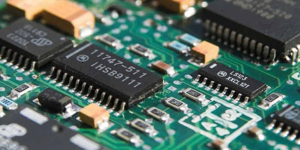
Modern electronics depend on printed circuit boards (PCBs). Still, when operating, they can produce a lot of heat. As a result, they affect the device’s functionality or even cause it to fail. So, designers and engineers use thermal relief PCBs. Specialized PCBs can dissipate heat produced by electronic components in their designs to lessen the impact of these issues. Consumer electronics, medical devices, aerospace, defense, and industrial environments depend on thermal relief PCBs.
Carefully considering pad size, copper trace width, via location, and efficient thermal dissipation is necessary when designing and implementing thermal relief PCBs. On the other hand, inadequate thermal relief PCB integration can lead to issues like weakened signal integrity, mismatched impedances, and increased EMI. In this article, we’ll go over the value of thermal relief PCBs in contemporary electronics, the difficulties and constraints that come with designing and using them, and the best methods for guaranteeing the performance and dependability of these specialty PCBs. We will also look at the many kinds of thermal relief pads, their advantages and disadvantages, and the uses of thermal relief PCBs across various sectors.
How thermal relief PCB works
A PCB design method known as thermal relief aids in controlling heat dissipation within the PCB. Adopting a pattern of copper traces and vias intended to lessen the amount of heat buildup in the board is the basis for the operation of thermal relief PCBs.
The main goal of thermal relief is to limit the quantity of copper that comes into contact with the component by establishing a link between the copper trace and the via. To accomplish this, the via rests on a pattern of tiny copper traces on a thermal relief pad.
The thermal relief pad decreases the heat transferred from a component to the rest of the PCB when soldered to the PCB. This is because the tiny copper traces act as a thermal barrier to stop heat from entering the copper trace, causing it to distort or expand.
Soldering the component to the PCB is also made simpler by the thermal relief pad. The pad has a bigger surface area for the solder to adhere to since it contains numerous tiny traces. This makes the connection between the component and the PCB stronger and more dependable.
Overall, the purpose of thermal relief PCBs is to lessen heat buildup within the PCB. Additionally, it establishes a more solid and dependable connection between the PCB and the component. Using this method, designers may produce better PCBs. This is because they can withstand high temperatures and are less prone to encounter issues like warping or component failure due to heat.
Importance of Thermal Relief PCB in PCB Design
Therm relief is a crucial PCB (Printed Circuit Board) design component. Therm relief is the connection between a copper pad or trace on a PCB and its component. A thermal relief pad is a small copper patch joined to a bigger copper patch by several delicate connections. To make it simpler to solder components to the PCB, these tiny connections are necessary.
The following list of factors illustrates the significance of thermal relief in PCB design:
Effective heat dissipation: Thermal relief aids in removing heat produced by PCB components. Thermal relief pads prevent overheating and guarantee that the component runs at a safe temperature. In addition, they supply a conduit for heat to escape from the component.
Soldering flaws, including voids and cold solder connections, are less likely to occur when using thermal relief pads. This is because the thermal relief pad’s small connections make it easier for the solder to flow around the pad and form a solid, dependable solder joint.
Easier rework: Thermal relief pads simplify removing or replacing a component if necessary. Removing the component without damaging the PCB or the other components on the board is simpler. We can attribute this to the tiny connections in the thermal relief pad.
Better signal integrity: By lowering the ground plane impedance, thermal relief pads can improve signal integrity. This results from the thermal relief pad’s narrow connections offering a less-resistive path to the ground. As a result, it lowers the ground plane impedance and enhances signal quality.
Determining the Size of the Thermal Relief Pad
The thermal relief pad’s size is essential when designing a printed circuit board (PCB). The thermal relief pad aids in transferring heat away from the component to which it is linked.
There are a few factors to consider when choosing the proper size of the thermal relief pad. One aspect is the size of the copper plane or trace to which the pad is linked. This aids in ensuring the even distribution of heat around the room. The component’s thermal requirements, linked to the pad, are another consideration. Ensuring the pad is big enough for sufficient heat dissipation from the component is crucial.
The thermal relief pad should have a diameter at least twice as large as the component lead or pad it connects to. However, the component’s thermal needs and the PCB design will determine the precise size. Additionally, it’s crucial to check that the thermal relief pad won’t increase the PCB’s cost or cause it to interact with other components.
In the end, careful consideration of several elements is necessary to determine the size of the thermal relief pad. You may ensure that your PCB performs at its peak levels by creating a suitable thermal relief pad.
The Importance of Copper Trace Width and Spacing

The copper traces’ width and spacing are ideal when designing a printed circuit board (PCB).
The copper trace’s width influences how much current it can carry, which prevents the PCB from overheating and failing. However, the trace might not be able to carry the necessary current if it is too small. Therefore, it’s crucial to base the width of the trace on the components’ present carrying capacities.
The distance between the copper traces also impacts the performance and dependability of the PCB. Electrical interference may negatively impact a board’s performance if the spacing is too close. Therefore, it’s crucial to design the spacing depending on the electrical needs of the PCB, considering signal integrity, noise, and impedance.
The copper trace width and spacing affect performance and the PCB’s manufacturing ability. For example, insufficient spacing could make it difficult or impossible to fabricate the PCB. In addition, it would cause delays and rework. Similarly, if the trace width is too small, it could be challenging to manufacture the copper layer with the necessary thickness.
The Impact of Via Placement on Thermal Relief PCBs
The positioning of vias can significantly affect the thermal performance of printed circuit boards (PCBs) with thermal relief. Vias are tiny holes drilled in the PCB that link the various layers of the board and permit the movement of heat and electrical impulses.
Via placement on thermal relief, PCBs can enhance the thermal performance of the board by supplying additional channels for heat to escape. In addition, adding vias all around the thermal pad can enable a quicker and more effective heat dissipation system. It allows quicker and more effective cooling.
Via placement, however, can potentially negatively affect the performance of the PCB if done incorrectly. Poorly positioned vias can produce thermal barriers obstructing the heat’s path. It results in hot spots and a possible board failure. In addition, a board’s structural integrity may damage, and the possibility of electrical shorts may increase if vias are too close together.
The thermal needs of the component and the PCB design must guarantee that the placement of vias on a thermal relief PCB is ideal. Furthermore, placement should guarantee that vias offer the required heat dissipation without impairing the board’s structural integrity or electrical performance.
Best Practices for Implementing Thermal Relief Pads
On a printed circuit board (PCB), thermal relief pads are a particular kind of copper plane separated from other copper traces to stop excessive heat from harming delicate components. The following advice will help you create and use heat relief pads successfully:
Ensure the thermal relief pad is the proper size to dissipate heat effectively. However, don’t let it be so large that it removes too much solder from the junction during the soldering operation.
Use trace width and spacing to prevent short circuits and other problems.
Utilize the recommended drill diameters, copper thicknesses, and solder mask clearances when designing PCBs.
Place the thermal relief pads strategically away from heat-sensitive components and close to high-power components.
Use suitable soldering procedures to ensure the thermal relief pads operate as intended.
Challenges and Limitations of Thermal Relief PCBs
Printed circuit boards (PCBs) with thermal relief can withstand high temperatures and lessen the likelihood of heat-related damage. Thermal relief PCBs do, however, have some restrictions and difficulties, just like any other technology. The primary issues and restrictions with thermal relief PCBs include the following.
Design Complexity: A complicated design with numerous vias is necessary for thermal relief PCBs. It can increase manufacturing complexity and expense. It may also be challenging to design the circuit board so that the thermal relief vias have enough room.
Limited Current Capacity: A PCB’s thermal relief vias may lower the circuit’s current capacity. It may be an issue for high-current applications. This constraint may impact the performance of the PCB in some applications.
Increased Impedance: Thermal relief vias may raise the circuit’s impedance, affecting the PCB’s performance. This impact is particularly prominent in high-frequency applications. A tiny increase in impedance might result in serious issues.
Reduced Reliability: By introducing weak spots where the board is more prone to malfunction or break, thermal relief vias in a PCB can lower the reliability of the circuit board. This is especially valid for uses where the PCB experiences significant vibration or stress.
Cost: Because of the complexity of the design and the additional materials needed to produce them, thermal relief PCBs are often more expensive than ordinary PCBs.
Thermal relief PCBs continue to be a popular option for high-temperature applications. Despite these difficulties and restrictions, they can provide considerable advantages in terms of performance and reliability. However, when selecting whether to employ a thermal relief PCB, it’s crucial to analyze the particular requirements of your application thoroughly.
Conclusion
Thermal relief PCBs are essential to the proper and long-term operation of electronic devices. They work by dispersing heat produced while various components are in use. If we don’t correctly manage this heat, it can cause damage and performance issues. This article emphasizes the significance of heat relief PCBs in various applications. They include consumer electronics, medical devices, aerospace and defense, and industrial settings. Designers and engineers can successfully include heat relief pads in PCB designs while navigating common challenges and limitations.
In conclusion, when developing thermal relief PCBs, many factors are essential. They consist of the dimensions of the pads, the copper trace width, the placement of the vias, and enough heat dissipation. Designers and engineers can prevent performance concerns since it ensures that their PCBs effectively control the heat produced by electrical components. It also increases the general dependability and toughness of their products. However, we must always consider the challenges and limitations of thermal relief PCBs.
