A Gerber file contains the data to design printed circuit boards (PCBs). It is a widely used file format in the sector. A 2D binary vector image file, Gerber files can display the copper layers, solder mask, and legend on PCBs.
The following details are in a Gerber file:
Copper layers: The copper traces, pads, and other features that will etch onto the PCB are in the copper layer in a Gerber file. For example, each line segment in a set of 2D vector graphics that make up the copper layer in a Gerber file represents a copper trace or pad. In addition, the copper traces’ width and spacing are in the Gerber file, along with any other pertinent design specifications like the pads’ size and shape. Usually, the PCB design software used to develop the PCB layout produces the Gerber file copper layer.
The copper traces: In the Gerber file, the copper traces are a collection of lines or curves that describe their size and shape. Essential characteristics that one must define in the Gerber file include the width and spacing of the copper traces. These factors depend on the specifications of the particular PCB design. The Gerber file also contains details on the layer stackup of the PCB.
Legend: The legend is the layer that includes details like part designators, reference designators, and other details that aid in PCB component identification. A layer in the Gerber file specifies the layout and location of the legend.
The de facto industry standard for PCB manufacture is the Gerber file extension, which is appropriate for almost all PCB fabrication software and production tools.
Importance of Gerber files in the manufacturing industry
Gerber files are a collection of files that include the information needed to create printed circuit boards (PCBs) for use in electronics production. Manufacturers worldwide utilize the Gerber file format as the industry standard for PCB design data.
Gerber files play a crucial role in manufacturing since they give designers and manufacturers a mechanism to exchange design information. For example, the board dimensions, layer stackup, copper traces, pads, vias, and drill holes are all included in the Gerber files, which also contain all the other information required to manufacture the PCB.
Representation of the accurate design: The PCB design, including the locations of copper traces, pads, and other components, is in Gerber files. This information is essential for the manufacturer to design an accurate and useful PCB.
The fabrication of PCBs now frequently uses Gerber files. It makes communication between manufacturers and designers straightforward. As a result, several vendors can now produce the same PCB design at the same quality.
Efficiency: Digital files with Gerber file extensions are simple to exchange, store, and edit. This digital format enables manufacturers to construct huge volumes of PCBs swiftly and correctly. In the process, they reduce the time and expense needed to create physical prototypes.
Automation: The various layers of the PCB include the copper layers, solder mask, and legend. One can automatically create them by manufacturing equipment using Gerber files. This automation increases the overall effectiveness of the production process. Additionally, it lowers the risk of errors.
A brief history of PCB Design
Printed circuit boards (PCBs) have been existing since the turn of the 20th century. However, using Gerber files in PCB design is a relatively recent innovation. A 2D vector graphic, a Gerber file, depicts a PCB design’s layout.
Before the invention of Gerber files, PCB designers produced actual artwork of the design that was then helpful in producing the PCB. However, designers could electronically construct PCB designs using CAD software. Gerber files allowed designers to submit their designs to PCB makers electronically. This happens after exporting them from one CAD application to another.
Over time, Gerber files have been expanding to contain more data. For example, they include drill, solder mask, and silkscreen data. Today, Gerber files are the famous format for sharing PCB design information between manufacturers and designers.
Gerber files are still commonly helpful and will remain crucial in PCB design. However, new formats like ODB++ offer advantages over Gerber files by containing more thorough design information.
Evolution of Gerber files
Since its development by Gerber Scientific Products, Inc. in the 1980s, Gerber files have been advancing significantly. Gerber files were initially helpful in exchanging PCB designs between various software packages and manufacturers.
At first, the only information in Gerber files related to a PCB design’s copper layers. However, the Gerber file format also advanced along with PCB technology. The Gerber file format now includes more layers like drill data, solder mask data, and silkscreen data.
The Gerber X2 format came into the market in the early 2000s. With this new format, all the information necessary for PCB manufacturers could be standardized and included in a single file.
Gerber files can now be helpful in new formats with even more sophisticated features. For instance, the ODB++ format has more precise design data that manufacturers can use to create more exact PCBs. Examples include a list of Gerber file extensions and component positioning information.
However, the industry continues to accept and use Gerber files widely. They are the ideal format for exchanging PCB design information between designers and producers. In addition, Gerber files continue to be the perfect file format for PCB designs used by many CAD software packages.
The Altium Gerber file extensions

Electronic designers frequently utilize Altium, a well-liked computer-aided design (CAD) program, to construct printed circuit boards (PCBs). However, once the design is complete, we must translate it into a language the PCB fabrication machinery can understand. The Gerber file extension is helpful in this situation. The industry-standard format for PCB fabrication is Gerber files, and Altium users can create these files in several other forms.
Each file extension has a distinct function necessary for fabricating a PCB. One must correctly generate them to produce a good PCB. Altium offers a complete set of tools for creating Gerber files. It lets you modify each layer and provide the board contour and drill information.
Gerber files can have several different file extensions, each serving a distinct function:
Gerber file extensions list
The top layer of copper traces, pads, and PCB design components are in the file with the extension.GTL (Top Copper Layer). Since it houses most of the circuitry, this layer is the most crucial on the PCB.
.GTS (Top Solder Mask Layer): This file provides the solder mask layer used to shield the copper traces on top of the PCB during assembly to avoid solder bridges.
The top overlay layer, or GTO (Top Overlay Layer), is the silkscreen layer printed onto the top of the PCB to denote component placement and polarity.
A paste mask layer utilized during solder paste is in the.GTP (Top Paste Mask Layer) file. This layer serves as a barrier to keep solder paste from getting on inappropriate surfaces.
The bottom layer of the PCB design’s copper traces, pads, and components are in the GBL (Bottom Copper Layer) file.
.GBS (Bottom Solder Mask Layer): This file provides the solder mask layer used to cover the copper traces at the bottom of the PCB during assembly. They protect them and avoid solder bridges.
The bottom overlay layer, the silkscreen layer printed onto the bottom of the PCB. It indicates component placement and polarity, which is in the file extension.GBO.
A paste mask layer used to apply solder paste to the bottom side of the board is in the file extension.GBP (Bottom Paste Mask Layer).
The GKO (Board Outline Layer) file contains the board outline layer. Once the panel is complete, the PCB comes from this layer.
Any additional mechanical information is in the GML (Mechanical Layer) file.
The drill data for the PCB is in the.TXT (NC Drill File) file. It includes any routing or milling instructions and details like the size and position of each hole.
Types of Gerber Files
There are several popular Gerber file types, including:
Top layer Gerber file
A top-layer Gerber file is an example of a file format helpful in producing printed circuit boards (PCBs). It includes a graphic depiction of the top layer of the PCB design in the common Gerber format for PCB manufacture.
The top layer Gerber file typically describes the position, size, shape, and orientation of all the components, traces, and other elements on the top layer of the PCB. Then, to transfer the design onto the top layer of the PCB during production, the PCB maker uses this information to generate a photomask.
There are typically other Gerber files besides the top layer Gerber file for the bottom layer, inner layers, and solder mask layers of the PCB. The PCB maker combines these files to produce the finished PCB.
Overall, the top layer Gerber file is essential to the PCB manufacturing process. It gives the manufacturer the data to create the PCB’s top layer following the original design parameters.
Bottom layer Gerber file
The Gerber file that contains the details for the copper traces and features on the bottom layer of the PCB is the “bottom layer Gerber file.” Typically, PCBs come in layers, each needing its own Gerber file.
The arrangement of components is all commonly part of the bottom layer Gerber file. The file might also have details on silkscreen layers and solder masks.
Manufacturers employ the Gerber files to build a photomask to transfer the circuit pattern onto a photosensitive material on the PCB. The undesired copper is subsequently removed with the help of the photomask, revealing the appropriate circuit layout.
Solder mask Gerber file
Soldering mask is the Gerber file format used during the printed circuit board (PCB) design process. It refers to the solder mask layer of the printed circuit board (PCB). This shield covers the copper traces to prevent the solder from contacting them during assembly.
The solder mask Gerber file specifies the size, shape, and location of the PCB areas the mask must cover. A producer makes a stencil from this information to apply solder mask material to the circuit board.
The solder mask Gerber file uses PCB design software, one of several needed for PCB manufacture. Additional files include the drill file, copper layers, and PCB layout.
Silkscreen Gerber file
Printed circuit boards (PCBs) use a type of file format called a silk screen Gerber file. The Gerber file format is a common format used to record the information found on the silk screen layer of a PCB. For example, it contains details about the positioning of components and other markings on the board.
Component outlines, part numbers, reference designators, and other data are printed directly into the PCB during manufacturing and are in a silk screen Gerber file. The Gerber file format is often helpful for exporting the file after creating it using software tools for designing PCB layouts.
It is crucial to have a silkscreen layer to ensure that components are appropriately on the PCB and that the board performs as intended. In addition, most PCB manufacturers support the Gerber file format, which is extensively helpful in electronics.
Drill file
Printed circuit boards (PCBs) use a type of file called a drill file, also referred to as an NC drill file. The drill file includes details about the PCB’s routing and slotting and the location and size of the holes that need drilling.
The drill file usually comes from the PCB layout software and exported in a format that PCB makers accept. This file includes details regarding the size, placement, and quantity of holes necessary for each location.
The drill file is a crucial part of the PCB manufacturing process since it contains the details required to drill the necessary holes in the appropriate places and sizes. Additionally, the drill file combines with other files, such as the Gerber files, to obtain a full set of manufacturing data for the PCB.
Drill files come in various forms, such as Sieb & Meyer and Excellon drill files. However, most PCB manufacturers support the Excellon format. Therefore, it is the most popular format for drill files.
Generating Gerber Files
The common format for describing printed circuit board (PCB) designs is Gerber files. There are numerous steps involved in creating Gerber files:
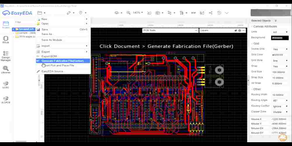
- PCB design software, such as Altium Designer or Eagle PCB, helps to create the PCB first. After that, component placement, trace routing, and copper layer construction are all part of the design.
- Produce Gerber files: The design program produces Gerber files after the PCB design is complete. Gerber files, which include copper layers, solder masks, and silkscreen, are image files that depict each printed circuit board layer (PCB).
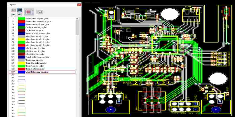
- Check the Gerber files: Next, we examine the Gerber files for errors or other problems using a Gerber viewer program. This ensures that the Altium Gerber file extensions appropriately represent the PCB design and that no layers are missing or overlapping.
- Submit Gerber files for manufacturing: Following their verification, the Gerber files go to the PCB manufacturer for production. The PCB will be made by the manufacturer using the Gerber files.
Overall, creating Gerber files is a crucial step in the PCB design process since it guarantees that the manufacturer will receive precise information about the design, leading to a high-quality PCB.
Gerber viewer tools
We can view and analyze the standard format used in the printed circuit board (PCB) industry, Gerber files using “Gerber viewer tools.” Engineers, designers, and producers that need to verify the accuracy of their PCB designs before putting them into production must have access to these technologies.
Here are some popular Gerber viewer tools:
You can read and analyze Gerber files with the free Gerbv viewer program on Linux, Mac OS X, and Windows systems.
ViewMate, a well-liked Gerber viewer tool from Pentalogix, offers a wealth of sophisticated tools for examining and manipulating Gerber files.
The free Gerber viewer program GC-Prevue offers simple analytical tools for calculating distances, angles, and areas. It also accepts a variety of file types.
A professional PCB design software package, Altium Designer, supports Altium Gerber file extensions.
Another well-liked PCB design software package with a Gerber viewer is Eagle PCB Design.
These are only a few of the numerous accessible Gerber viewing tools. Consider the functionality you require, the platform you use, and whether you want a free or premium solution when selecting a Gerber viewer tool.
