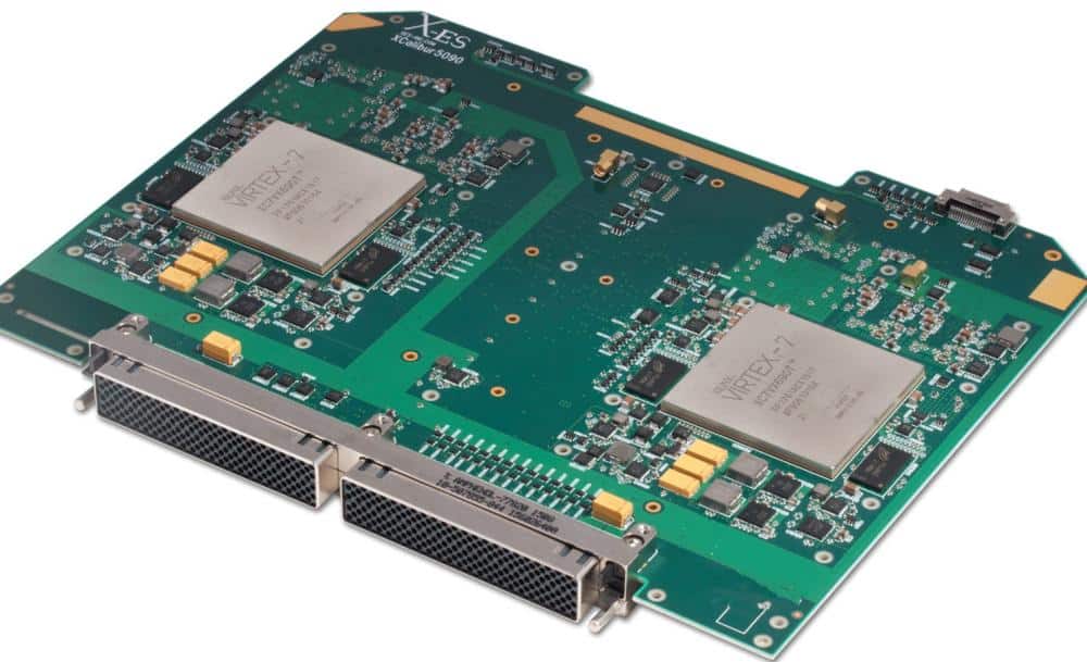
The aerospace and defense industry are constantly faced with various challenges. One of these challenges is how to offer enhanced functionality while providing smaller systems. This particular challenge resulted in the development of the Xilinx Defense-grade Zynq-7000Q SoC.
The defense-grade Zynq-7000Q family is suitable for applications that need advanced system control. Also, they are specifically designed for applications demanding advanced digital signal processing. The Xilinx Defense-grade Zynq-7000Q SoC has a lot to offer. The on-chip programmable logic offers a cost-effective means to meet current security mandates. Therefore, this article provides in-depth information on the defense-grade Zynq-7000Q SoC.
————————————————————————————
Request Xilinx Defense-grade Zynq-7000Q FPGA Quote , Pls Send PCB Files to Sales@raypcb.com Now
————————————————————————————
What is the Function of the Xilinx Defense-grade Zynq-7000Q SoC?
The Xilinx Defense-grade Zynq-7000Q SoC provides the scalability and flexibility of an FPGA. This family offers performance and ease of use related to ASSPs and ASICs. The Xilinx Defense-grade Zynq-7000Q SoC comprises various devices. Therefore, these devices enable designers to target high-performance applications. Designers use industry-standard tools to achieve this.
Every device in the Defense-grade Zynq-7000Q SoC comprises the same I/O, PS, and PL. However, there is a variation in the resources available in these devices. Therefore, the Defense-grade Zynq-7000Q SoC is ideal for different applications in extreme conditions. These applications are:
- Targeting and tracking
- Surround View
- Displays
- Sensor and Radar processing
- Synthetic vision
- Displays
- Image fusion and processing
- Multi-spectral imaging
The Defense-grade Zynq-7000Q SoC allows custom logic implementation in the PS and PL. also, it enables the realization of differential system functions. The integration of the PL with the PS enables a performance level that two-chip solutions can’t match. This incompatibility is a result of their limited power budget and I/O bandwidth.
The Defense-grade Zynq-7000Q SoC features a wide range of soft IPs. There are Linux device drivers for the peripherals in the PL and PS. The development environment of the Vivado Design Suite allows a rapid product design for hardware and software. The implementation of the ARM-based PS brings a variety of third-party tools. Also, it brings IP providers with the existing PL ecosystem of Xilinx.
There is high-level operating system support due to the addition of an application processor. Also, there are other standard operating systems utilized with the Cortex-A9 processor. This is for the Defense-grade Zynq-7000Q series.
The Description of Processor System (PS)
The processor system consists of four major blocks which are:
- Memory interfaces
- Interconnect
- Application processor unit (APU)
- I/O peripherals (IOP)
Memory interfaces
There are static memory interfaces and a dynamic memory controller in this interface. The static memory controllers support a parallel data bus and a NAND flash interface. Also, the dynamic memory controller provides support for DDR2, DDR3, LPDDR2, and DDR3L memories. The dynamic memory controller allows the PL and the PS to access a common memory. Also, the DDR controller comprises four AXI slave ports.
The static memory interfaces provide support for external static memories like:
- 2-bit SPI, 1-bit SPI, and 2-bit SPI
- 8-bit SRAM data bust that supports about 64 MB
- ONFi 1.0 NAND flash support
- 8-bit parallel NOR flash that supports about 64 MB
Interconnect
All other blocks in the processor system are well-connected to each other except the interconnect. The other three blocks connect to each other and to the PL via a multilayered ARM AMBA AXI interconnect. However, the Interconnect supports several simultaneous master-slave transactions. Also, the interconnect features latency-sensitive masters like ARM CPU. Therefore, the interconnect has the shortest paths to bandwidth critical masters and memory.
You can regulate the traffic through the Interconnect via the Quality of Service (QoS) block in the Interconnect. Also, the QoS feature regulates traffic produced by the DMA controller and the CPU.
————————————————————————————
Request Xilinx Defense-grade Zynq-7000Q FPGA Quote , Pls Send PCB Files to Sales@raypcb.com Now
————————————————————————————
The Application Processor Unit (APU)
The APU has dual-core ARM Cortex-A9 MP Cores. Each of these cores has 2.5 DMIPS/MHZ. Also, each core can operate in a symmetric dual processor and a single processor. The accelerator coherency port (ACP) interface allows coherent access from PL to the CPU. The APU features TrustZone which enables secure operation. Also, there are three watchdog timers for each CPU. There are also two triple timers/counters (TTC) and a general interrupt controller (GIC).
The I/O peripherals (IOP)
The I/O peripherals unit features a data communication peripheral. Therefore, the major features of the IOP are:
- Two UARTs
- About 118 GPIO bits
- Two full CAN2.OB compliant CAN
- Two USB 2.0 OTG peripherals, which support about 12 endpoints
- Two full-duplex SPI ports with three peripherals chip select
A shared pool of 54 dedicated multiple-use I/O pins helps the IOP peripherals to relate to external devices. Every peripheral can get one of the pre-defined groups of pins. Therefore, this enables a flexible assignment of several devices simultaneously. 54 pins aren’t adequate for simultaneous use of all IOP peripherals. However, the majority of IOP interface signals aren’t available to the PL. Therefore, this enables the use of standard PL I/O pins when they are well configured. Also, all MIO pins provide support for 1.8V LVCMOS and HSTL standards.
The Programmable Logic (PL) Description
The programmable Logic features some major components. These components are:
- 36 kb Block RAM
- Programmable I/O Blocks
- CLB
- Two 12-bit XADC
- Low-power serial transceivers in Zynq-7000 SoCs
- DSP slices
Each of these components will be reviewed in this section.
Block RAM
The Block RAM is an essential component in the Programmable Logic. This is a 36 Kb block RAM with about 72 port widths. It has a built-in error correction circuitry which is optional. Also, it features programmable FIFO logic. Each Defense-grade Zynq-7000Q device comprises 140 and 755 dual-port block RAMs. Also, each store about 36 Kb. Furthermore, every block RAM features two independent ports that share the stored data.
- Programmable data width
It is possible to configure every port as 4K x 9 (or 8), 32K x 1, or 8K x 4. Also, the two ports can feature aspect ratios with no constraints. It is possible to divide each block RAM into two independent 18 Kb block RAMs.
You can only access data widths above 18 bits or 36 bit in simple dual-port. Therefore, this mode dedicates one port to read operation. While the other port writes operation. In the simple dual-port mode, one side can be variable. The other side can be fixed to 64/72 or 32/36. The two sides of the dual-port 36 Kb RAM can have different widths.
- FIFO controller
The FIFO controller for synchronous or asynchronous operation increases the internal addresses. Also, it offers four hand shaking flags. These flags are almost full, full, almost empty, and empty. The almost empty and almost full flags are programmable. Also, the FIFO depth and width are programmable. However, the read and write ports feature identical widths.
- Error identification and correction
Every 64-bit wide block RAM can store, produce, and use eight extra Hamming code bits. It can detect the double-bit error. Also, it can correct the single-bit error during the read process.
Programmable I/O blocks
The programmable logic I/O feature the following
- High-frequency decoupling capacitors for increased signal integrity
- High-performance SelectIO technology for 1866 Mb/s DDR3 support
- Digitally controlled impedance
The device and package size determine the number of I/O pins. Every I/O can comply with a huge number of I/O standards. Also, each I/O is configurable. All other PL pins feature similar I/O capabilities. These capabilities can be constrained by some banking rules. Therefore, the Select IO resources in Zynq-7000Q are High Performance or High Range.
The High Performance I/Os operates on high performance from 1.2V to 1.8V. The High Range I/Os provide the highest voltage support which ranges from 1.2V to 3.3V. All I/O pins are properly organized in banks. Also, there are 50 pins for each bank. Every bank features a common Vcco output supply.
The Defense-grade Zynq-7000Q utilizes a wide range of package types to meet the demands of the user. Therefore, this includes a small form factor for high-performance flip-chip packages. Also, the silicon uses a high-performance flip-chip process to attach to the package substrate.
I/O Logic
- Output and Input Delay
It is possible to configure all outputs and inputs as registered or combinatorial. All inputs and outputs support Double data rate (DDR). Some outputs and inputs can be separately delayed by about 32 increments of 52 ps or 78ps each. These kinds of delays are ideally implemented as ODELAY and IDELAY. Also, you can set the number of delay steps by configuration.
- OSERDES and ISERDES
Several applications combine bit-serial I/O with a much slower parallel function. Therefore, this needs a deserializer and serializer (SerDes) in the I/O structure. Every I/O pin has an 8-bit ISERDES and OSERDES that can perform parallel-to-serial or serial-to-parallel conversions.
————————————————————————————
Request Xilinx Defense-grade Zynq-7000Q FPGA Quote , Pls Send PCB Files to Sales@raypcb.com Now
————————————————————————————
Configurable Logic Block (CLB)
The CLB features 6-input Look-Up tables (LUTs) and memory capability within the LUT. Also, this block has shift register and register functionality. In the Defense-grade Zynq-7000Q SoCs, you can configure the LUTs as one 6-input LUT with an output. Also, you can configure the LUTs as two 5-input LUTs with distinct outputs but similar addresses.
You can register every LUT in a flip-flop. Therefore, such LUTs and their flip-flops form a slice.
XADC (Analog-to-Digital Converter)
The XADC features the following:
- On-chip power supply and temperature sensors
- About 17 user-configurable analog inputs
- On-chip reference option
- JTAG access to ADC measurements
- Dual 12-bit 1 MSPS ADCs
Defense-grade Zynq-7000Q SoCs implement an analog interface known as XADC. This analog interface can address a wide range of data acquisition when combined with the PL capability. Also, it can address monitoring requirements.
There are two 12-bit 1 MSPS ADCs with different track and hold amplifiers in the XADC. Also, the XADC features an on-chip supply and thermal sensors and an on-chip analog multiplexer. The on-chip reference circuit is optionally utilized by the XADC. Therefore, it removes the need for external active components.
An external 1.25V reference IC is crucial to achieving the full 12-bit performance of the ADCs. Furthermore, the XADC digitizes the on-ship sensors’ output if it isn’t instantiated in a design. The latest measurement results are well-stored in registers for access. The user-defined alarm thresholds can specify unacceptable power supply variation. Also, it can indicate over-temperature events. A user-specified limit can help to start an automatic power-down.
Low-power Serial Transceivers
The transceiver counts in the Defense-grade Zynq-7000Q SoCs range from 0 to 16 transceiver circuits. Every serial transceiver features a receiver and transmitter. The different Zynq-7000 serial transceivers can combine LC tank architecture and ring oscillators. Therefore, this enables the combination of functionality and flexibility. Also, it allows IP portability across the devices.
The Zynq-700 logic-based oversampling can help to achieve lower data rates. The serial receiver and transmitter are independent circuits using an optimized PLL architecture. Every transceiver comprises a wide range of user-definable parameters and features. Therefore, you can define all of these during the configuration of the device.
Receiver
This is a serial-to-parallel converter. Therefore, transforms the incoming bit-serial differential signal to a parallel stream of words. The receiver gets the incoming differential data stream and feeds it via programmable linear. The data pattern utilizes non-return-to-zero encoding. Also, it assures adequate data transition by utilizing the selected encoding scheme. The RXUSRCLK clock then helps to transfer parallel data into the PL. The transceivers provide a special low power mode for further power reduction.
Transmitter
This is a parallel-to-serial converter. The transmitter features a conversion ratio of 80,64, 32, 40, 20, or 16. Therefore, a single-channel differential output signal helps the transmitter output to drive the PC board.
Out-of-band signaling
The out-of-band (OOB) signaling is primarily offered by the transceivers. Therefore, this helps to send low-speed signals to the receiver. At this point, the low-speed serial data transmission is inactive. This is possible when the link hasn’t been initialized. SATA/ SAS and PCI Express applications can benefit from this.
Digital Signal Processing – DSP Slice
The DSP Slice offers these functions:
- Optimization of symmetrical filter applications through power-saving pre-adder
- 25 x 18 two’s complement accumulator high-resolution signal processor
DSP applications utilize several binary accumulators and multipliers, best used in dedicated DSP slices. All devices in Defense-grade Zynq-7000Q feature low-power DSP slices. These slices combine high speed with small size. Furthermore, they retain system design flexibility.
Every DSP slice features a 48-bit accumulator and a dedicated 25 x 18 bit two’s complement multiplier. Both components can operate up to 650 MHz. The two 48-bit inputs can feed a logic unit that can produce any of the ten logic functions. There is an additional pre-adder in the DSP. Also, this pre-adder is typically utilized in symmetrical filters. Furthermore, it enhances performance and functionality in densely packed designs. It can also minimize the DSP slice count by 0.5.
In addition, there is a 48-bit wide Pattern Detector in the DSP. This Detector is ideal for symmetric or convergent rounding. Also, the pattern detector can implement 96-bit-wide logic functions when used with the logic unit. Therefore, the DSP slice offers extension capabilities that improve the efficiency of applications beyond digital signal processing. These applications include:
- memory-mapped I/O register files
- memory address generators
- Wide dynamic bus shifters
- Wide bus multiplexers
Defense-grade Zynq-7000Q SoC Devices
The Defense-grade Zynq-7000Q SoC has several devices. Each of these devices has unique features. These devices are suitable for defense and space applications.
XQ7Z045-2RF676I XQ7Z045-1RF676Q XQ7Z030-1RF676Q
XQ7Z020-1CL484I XQ7Z100-2RF900I XQ7Z100-1RF1156I
XQ72020-CL484
Features of XQ7Z045-2RF676I
- It has anti-counterfeiting features
- Also, it comes with CPU frequency of about 800 MHz
- Supports Byte-parity
- Comprises one global timer and three watchdog timer
- Also, it comes with fully leaded content
- It has 2.5 DMIPS/MHz for each CPU
- Furthermore, it comprises multiprotocol dynamic memory controller
- Has static memory interfaces
- ECC support in 16-bit mode
- Also, it comes with TrustZone security and Thumb-2 instruction set
- It recognizes 1588 rev. 2 PTP frames
- Also, it has an 8-bit ULPI external PHY interface
- It supports high-speed and low-speed modes
- Furthermore, it has got Intel EHCI compliant USB host
- It has about 16 transmitters and receivers
- Features IEEE Std 1149.1 Compatible Test Interface
- It supports parallel NOR flash and ONFI1.0 NAND flash
- Has full-duplex SPI ports
- Comes with two high-speed UARTs and two master and slave 12C interfaces
- Also, it comprises On-chip boot ROM and 256KB on-chip RAM
————————————————————————————
Request Xilinx Defense-grade Zynq-7000Q FPGA Quote , Pls Send PCB Files to Sales@raypcb.com Now
————————————————————————————
Features of XQ7Z045-1RF676Q
The XQ7Z045-1RF676Q comprises the following features:
- Full-range temperature testing
- It comes with NEON media-processing engine and Program Trace Macrocell (PTM)
- Also, it has two triple-timer counters Caches
- The CPU frequency is about 800 MHz
- Also, it comes with 25-bit pre-adder and 48-bit adder
- It supports LVDS, SSTL, and LVCMOS
- Furthermore, it comes in IEEE Std 1149.1 interface
- It supports about Gen2 speeds and about 8 lanes
- Also, it comprises about 17 external differential input channels
- Has on-chip temperature sensing and voltage
- Also, it comes with GPIO with four banks
- It supports parallel NOR flash and ONFI1.0 NAND flash
- There are 54 flexible multiplexed I/O for peripheral pin interconnect
- Also, it features cascadable adders, Look-up tables and flip-flops
- It has static memory interfaces
- Also, it has the ability to recognize 1588 rev. 2 PTP frames
- It supports low-speed, on-the-go speed, and high-speed modes
Features of XQ7Z030-1RF676Q
- Has ruggedized packaging and fully leaded content
- Comes with anti-tamper support
- Also, it assures fourth-generation information
- Has Vector Floating Point Unit (VFPU)
- Also, it comprises three watchdog timers and one global timer
- Has byte-parity support and static memory interfaces
- Also, it comes with 2-bit SPI, 1-bit SPI, and 4-bit SPI
- It comes with USB 2.0 compliant device IP core
- Also, it comprises flip-flops and cascadable adders
- Has two SD/SDIO 2.0 compliant controllers
- Comes in master and slave 12C interfaces
- It supports both high-speed and low-speed modes
- Also, it supports about 10. 3125 Gb/s data rates
- It supports parallel NOR flash and ONFI1.0 NAND flash
- Has about 17 external differential input channels
- It is about 72 bits wide and has true Dual-port
- Also, it can identify 1588 rev. 2 PTP frames
- Furthermore, there are 54 flexible multiplexed I/O for peripheral pin interconnect
Features of XQ7Z020-1CL484I
- It supports high-speed and low-speed modes
- Furthermore, it has got Intel EHCI compliant USB host
- It has about 16 transmitters and receivers
- Features IEEE Std 1149.1 Compatible Test Interface
- Has full-duplex SPI ports
- Comes with two high-speed UARTs and two master and slave 12C interfaces
- Also, it comprises On-chip boot ROM and 256KB on-chip RAM
- It has 2.5 DMIPS/MHz for each CPU
- Furthermore, it comprises multiprotocol dynamic memory controller
- Has static memory interfaces
- ECC support in 16-bit mode
- Also, it comes with TrustZone security and Thumb-2 instruction set
- It recognizes 1588 rev. 2 PTP frames
- Also, it has an 8-bit ULPI external PHY interface
- It has anti-counterfeiting features
- Also, it comes with CPU frequency of about 800 MHz
- Supports Byte-parity
- Comprises one global timer and three watchdog timer
- It supports parallel NOR flash and ONFI1.0 NAND flash
- Also, it comes with fully loadedcontent
Features of XQ7Z100-2RF900I
- It comes with NEON media-processing engine and Program Trace Macrocell (PTM)
- Full-range temperature testing
- Also, it has two triple-timer counters Caches
- The CPU frequency is about 800 MHz
- Also, it comes with 25-bit pre-adder and 48-bit adder
- It supports LVDS, SSTL, and LVCMOS
- Furthermore, it comes in IEEE Std 1149.1 interface
- It supports about Gen2 speeds and about 8 lanes
- Also, it comprises about 17 external differential input channels
- Has on-chip temperature sensing and voltage
- Also, it comes with GPIO with four banks
- There are 54 flexible multiplexed I/O for peripheral pin interconnect
- It supports parallel NOR flash and ONFI1.0 NAND flash
- Also, it features cascadable adders, Look-up tables and flip-flops
- It has static memory interfaces
- Also, it has the ability to recognize 1588 rev. 2 PTP frames
- It supports low-speed, on-the-go speed, and high-speed modes
- Furthermore, it gets rid of ASSP-FPGA bottleneck
Features of XQ7Z100-1RF1156I
- Has Vector Floating Point Unit (VFPU)
- Also, it comprises three watchdog timers and one global timer
- Has byte-parity support and static memory interfaces
- Has ruggedized packaging and fully leaded content
- Comes with anti-tamper support
- Also, it assures fourth-generation information
- Has two SD/SDIO 2.0 compliant controllers
- Comes in master and slave 12C interfaces
- Also, it comes with 2-bit SPI, 1-bit SPI, and 4-bit SPI
- It comes with USB 2.0 compliant device IP core
- Also, it comprises flip-flops and cascadable adders
- It supports both high-speed and low-speed modes
- Also, it supports about 10. 3125 Gb/s data rates
- It supports parallel NOR flash and ONFI1.0 NAND flash
- Has about 17 external differential input channels
- It has several processing solution in one device
- Furthermore, there are 54 flexible multiplexed I/O for peripheral pin interconnect
- It is about 72 bits wide and has true Dual-port
- Also, it can identify 1588 rev. 2 PTP frames
————————————————————————————
Request Xilinx Defense-grade Zynq-7000Q FPGA Quote , Pls Send PCB Files to Sales@raypcb.com Now
————————————————————————————
Features of XQ72020-CL484
- It has about 16 transmitters and receivers
- It supports high-speed and low-speed modes
- Furthermore, it has got Intel EHCI compliant USB host
- Features IEEE Std 1149.1 Compatible Test Interface
- Has full-duplex SPI ports
- Comes with two high-speed UARTs and two master and slave 12C interfaces
- Also, it comprises On-chip boot ROM and 256KB on-chip RAM
- It has 2.5 DMIPS/MHz for each CPU
- Furthermore, it comprises multiprotocol dynamic memory controller
- Has static memory interfaces
- ECC support in 16-bit mode
- Also, it comes with TrustZone security and Thumb-2 instruction set
- It recognizes 1588 rev. 2 PTP frames
- Also, it has an 8-bit ULPI external PHY interface
- It has anti-counterfeiting features
- Also, it comes with CPU frequency of about 800 MHz
- Supports Byte-parity
- Comprises one global timer and three watchdog timer
- Also, it comes with fully leaded content
- It supports parallel NOR flash and ONFI1.0 NAND flash
Conclusion
The Defense-grade Zynq-7000Q family is specifically based on the architecture of the Xilinx Soc. These devices incorporate a 28 nm Xilinx PL and a dual-core ARM Cortex-A9 based PS in a single device. Therefore, this is ideal for extreme environment applications like Defense and Aerospace.
Furthermore, the PL and the PS are on distinct power domains. Therefore, this allows users to power down the PL for any power management. Also, the processors in the PS will boot first. This enables a software-centric approach for the configuration of PL. The software running on the CPU helps to manage PL configuration. Therefore, it boots like an ASSP.
