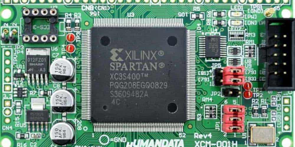
Xilinx designed the XC3000 Series FPGAs to provide digital integrated circuits. The Program data stays externally in a ROM, EPROM, or EEPROM. Configuration PROMs offer serial configuration program storage. In this article, we will have an in-depth look into Xilinx XC3000 Series FPGAs.
XC3000 Series FPGAs – What is it?
The XC3000 Series FPGAs offer a group of high-density digital integrated circuits. The user-programmable array architecture of this series features a configuration program store. Also, there are three different types of configurable elements. These elements are:
- An array of configurable Logic Blocks (CLBs)
- A perimeter of Input/Output blocks
- Resources for interconnection
The development system offers schematic capture for design entry. Also, it provides auto place-and-route. There are design verification alternatives such as the in-circuit emulation and logic and timing simulation. The design editor helps interactive design optimization. Also, it compiles the pattern representing the configuration program.
In addition, the configuration program data store in internal static memory cells. These data determine the LCA user logic interconnections and functions. Xilinx XC3000 series FPGAs offer various logic capacities and speed grades.
The Configuration Memory
The static memory cell in the Logic Cell Array was specifically designed for high reliability. Also, it allows noise immunity. Static memory offers high density and comprehensive testability. Furthermore, the basic memory cell features two CMOS inverters and a pass transistor. The pass transistor helps to read and write cell data. However, you can only write the cell during configuration. Also, you can read the cell during readback.
The cell offers continuous control during normal operation. Also, the pass transistor remains off and won’t affect cell stability. However, this is different from the operation of conventional memory devices. In these devices, the cells are often rewritten and read.
The extreme power-supply excursion doesn’t affect the configuration memory cells. This is because of their structure. No soft defects occurred in the presence of high doses of alpha radiation. There are different methods of loading the data. Some methods utilize serial data while others use byte-wide data.
——————————————————————————————————————
Request Xilinx XC3000 Series FPGA, Pls Send Files to Sales@raypcb.com Now
——————————————————————————————————————
I/O Block
Every user-configurable IOB offers an interface between the internal user logic and the external package pin. Also, there are direct input and registered paths in each IOB. Every IOB offers a programmable 3-state buffer. A director-registered output signal may drive this buffer. Configuration options enable every IOB an inversion and a high-impedance pull-up. Also, each input circuit offers input clamping diodes to enable electrostatic protection.
The input buffer part of every IOB offers threshold detection. Therefore, this helps to translate external signals applied to the package pin. You can program the global input-buffer threshold of the IOB. This input-buffer of the IOBs can be either programmed to work with CMOS or TTL levels. The clocking polarity is programmable for every clock line on each of the four die edges.
Inputs need transition times of < 100 ns and shouldn’t be left floating. Furthermore, floating CMOS input-pin circuits might produce oscillations. This is because these circuits might be at a threshold. Every user IOB contains a programmable high-impedance pull-up resistor. The Logic Cell Array (LCA) offers circuitry for input protection of electrostatic discharge. However, it is important to observe normal CMOS handling precautions.
IOB flip-flop loop delays are almost 3 ns. This delay offers great performance under asynchronous data and clock conditions. In addition, short loop delays reduce the possibility of a metastable condition. This condition can be due to the clock’s assertion during data transmissions. The IOB flip-flops can synchronize external signals attached to the device. This can be a result of the short-loop delay characteristics in the LCA.
You can use the signals internally without considering their clock relative timing. However, if it applies to the routing-path delays and internal logic, the signals can’t be used.
The Configurable Logic Block of Xilinx XC3000 Series FPGAs
The configurable logic block (CLB) offers functional elements. The logic blocks are well-arranged in a matrix within the IOBs’ perimeter. Also, the XACT development system compiles the configuration data. You need to load this data into the configuration memory. Therefore, this will help to specify the interconnection and operation of each block.
Every CLB features two flip-flops and a combinatorial logic section. Also, there are two outputs in each CLB. These outputs (x and Y) may drive interconnect networks. The function G or F outputs of the combinatorial logic supplies data input within a CLB. The RESET pin or active-Low chip input resets all flip-flops. Also, the flip-flops might reset during the configuration process.
In addition, the flip-flops share the EC. When the EC is low, it recirculates the present states of the flip-flop. Also, it inhibits response to the combinatorial function inputs on a CLB. The CLB’s combinatorial-logic portion utilizes a 32 by 1 LUT to execute Boolean functions. LUT means Look-Up table. The variables from the two internal block flip-flops are the table address inputs.
Types of Modes in the Xilinx XC3000 Series FPGAs
The Xilinx XC3000 Series FPGAs feature different kinds of modes. Each of these modes has its unique functions:
Peripheral Mode
This mode offers a simplified interface via which the device may load byte-wide. The LCA device produces a configuration clock from the timing generator. The peripheral mode can serve as a lead device for slave devices.
Master mode
The LCA device loads the configuration data automatically in Master Mode. This mode utilizes serial configuration data delivered to Data-in from a synchronous serial source. The Master Parallel High and Low modes use parallel data sent to the D0-D7 pins.
Slave Serial Mode
This mode offers a very simple interface for loading LCA configuration. Here, the serial data transmit in line with a synchronizing input clock. Also, the majority of slave mode applications are in daisy chain configurations. Also, a processor can supply data.
Configuration Functions
The configuration data has control over different special functions. These functions are:
- Input thresholds
- RESET timing
- Readback disable
- Oscillator frequency division
- DONE timing
- DONE pull-up resistor
The configuration data bits control each of these functions. These bits are part of the XACT development system bitstream.
Input thresholds
Before completing all configurations, all LCA input thresholds must be TTL compatible. The input thresholds are either CMOS or TTL compatible after the configuration completion. TTL threshold option needs some extra supply current for threshold shifting. Before completing the configuration, the user I/O pins have a high-impedance pull-up. Also, the configuration program can enable the IOB pull-up resistors to function as input load.
RESET Timing
A selection in the MakeBits program can control the timing of the launch of the internal reset. The RESET keeps programmable latches and flip-flops in a zero state.
Readback
If a bitstream programs with an LCA, you have to read back the contents. Readback can serve as a way of verifying the configuration. Also, it can serve as a way of determining the condition of internal logic nodes. There are three different options to generate the configuration bitstream:
- On commandenables unrestricted use of Readback
- Never possesses the Readback capability
- One-timeholds Readback after executing a Readback to confirm the configuration
You can achieve Readback without using any user I/O pins. Also, you need only CCLK, M1, and M0. Readback data comprises the present state of every CLB flip-flop and each device pad. These data are into unused configuration bit during Readback.
Oscillator division
A selection in the MakeBits program can enable the user to implement a divide-by-two flip-flop. Also, this flip-flop will be between the alternate clock lie and the crystal oscillator. Therefore, this ensures there is a symmetrical clock signal.
DONE Timing
A selection in the MakeBits program can occur as a CCLK cycle after or before the outputs are active. This will help to control the timing of the DONE signal.
——————————————————————————————————————
Request Xilinx XC3000 Series FPGA, Pls Send Files to Sales@raypcb.com Now
——————————————————————————————————————
How Does the Xilinx XC3000 Series FPGAs Function?
The Xilinx XC3000 Series FPGAs can achieve great performance through:
- The development and enhancement of the sub-micron manufacturing process for producing CMOS SRAMs
- Careful increment of transistor geometries, lay-out, and circuit design
- A look-up table that can collapse multi-layer combinatorial logic in a function generator. One CLB can use about four layers of conventional logic in 2.7 ns.
The timing of critical paths determines the actual system performance. The specifications of AC-timing reveal the worst-case timing parameters for the different logic resources in XC3000 FPGAs.
General Features of the Xilinx XC3000 Series FPGAs
The Xilinx XC3000 Series FPGAs feature five related FPGA families. Also, they have got some exceptional features like:
- Unlimited reprogrammability
- Complete XACT Development System
- They are suitable for different custom VLSI design tasks
- High-performance CMOS static memory technology
- Ideal for volume production
- Flexible FPGA architecture
Also, they have expensive packaging options
Pin Descriptions in XC3000 Series
There are different types of pins on the XC3000 series FPGAs. Each pin has its own functions.
INIT
This active Low open-drain output features a weak pull-up. Therefore, it is Low during the internal clearing of the configuration memory. Also, the INIT pin becomes an I/O pin after configuration.
GND
This pin ranges from two to eight. The number of pins used depends on the type of package. All GND pins must connect to the ground.
RESET
This pin has three functions. Before configuration, the configuration process will experience a delay. An internal circuit will begin a reduced time-out cycle when it senses power application. The LCA device will restart the configuration at the cancellation of RESET. This happens if RESET asserts during the configuration process. If RESET asserts after the configuration process, it offers a global asynchronous RESET of IOBs.
M2
This input features a weak pull-up resistor during configuration. M2 pin becomes an I/O pin after configuration.
DIN
DIN pin serves as a serial-data input during Master or Slave serial configuration. This is the DATA of input in the Peripheral or Master configuration. Also, this pin will become an I/O pin after the completion of a configuration.
BUSY
The BUSY pin specifies when the chip is available for it to accept another written byte of data. Also, this pin will become an I/O pin upon completion of the configuration.
HDC
This output is at a High Level when the configuration isn’t yet complete. The HDC pin will be a user-programmable I/O pin upon configuration completion.
DONE
This is an open-drain output. DONE is configurable without or with an internal pull-up resistor. The LCA device circuitry will be active in a synchronous order after configuration. Also, DONE will be active High one cycle after or before the outputs become active. After configuration, a High-to-Low transition will result in the initialization of the LCA device.
Types of Metal Resources for Various Network Interconnect Requirements
Direct interconnect
This offers the most effective implementation of networks between I/O or CLBs. Signals that use direct interconnect have low interconnect propagation. Also, these signals use no general interconnect resources. For every CLB, the X output may be directly linked to the B input of the CLB.
General Purpose interconnect
This comprises a grid of five vertical and five horizontal metal segments. These segments are between the columns and rows of IOBs and logic. Each segment is the width or height of a logic block. You can join the ends of these segments by switching matrices. Also, this enables programmed interconnections between the segments of adjoining columns and rows.
Longlines
Longlines go past the switch matrices. They are primarily meant for signals traveling a long distance. Longlines run horizontally and vertically the width or height of the interconnect area. Every interconnect row features two horizontal longlines. However, each interconnect column comprises three vertical longlines. Also, the additional longlines are adjacent to the outer parts of the switching matrices.
An IOB output or a logic block can drive longlines on a column-by-column basis. Therefore, this offers a low skew control within every column of logic blocks.
XC3000 Series FPGAs Devices
The devices below belong to the XC3000 series FPGAs. Each of these devices has its unique features.
XC3195A-5PQ208I XC3195A-4PC84I XC3195A-4PQ160I
XC3195A-3PCG84C XC3195A-3PP175C XC3195A-3PC84C
XC3195A-2PC84C XC3190A-PQ160AKJ XC3195A-2PQ160I
XC3190A-4PQ208C XC3190A-4PQ160C XC3190A-4PQ160I
XC3190A-4PC84C XC3190A-3PC84C XC3190A-3PQ208C
XC3164A-4PQ160C XC3190-3PQ208C XC3164A-4PC84C
XC3164A-3TQ144C XC3142A-4PQ100C XC3142A-5PC84C
XC3142A-3PQG100C XC3142A-3PQ100I XC3142A-4PC84C
XC3142A-3PQ100C XC3130A-4PQ100C XC3142A-2PQ100I
XC3130A-3VQ100C XC3130A-4PC68C XC3130A-3PQ100C
XC3130A-2VQ100C XC3130A-3PC84C XC3130A-2PC44C
XC3130A-1PC84C XC3130A-1PCG68C XC3130A-09PQ100C
XC3120A-3PC68C XC3120A-4PQ100C XC3090A-7PQ160I
XC3090A-7PC84I XC3090A-7PC84C XC3090A-7PG175M
XC3090-70PP175C XC3090-7PQ160C XC3090-70PG175C
XC3090-70PG175B XC3090-100PP175C XC3090-70PC84C
XC3064A-7TQG144I XC3090-100PG175C XC3064A-7TQ144I
XC3064A-7PQ160C XC3064A-7PC84I XC3064A-7TQ144C
XC3064-70PP132C XC3064A-7PC84C XC3064-70PC84I
XC3064-100PP132IQ XC3064-100PQ160C XC3064-100PG132I
XC3042A-7VQ100C XC3042L-8VQ100I XC3042A-7TQ144C
XC3042A-7PQG100I XC3042A-7PQ100C XC3042A-7PQ100I
XC3042A-7PG84M XC3042A-7PG84I XC3042A-7PP132I
XC3042A-7PG132I XC3042A-7PC84C XC3042A-7PC84I
XC3042A-6TQ144C XC3042A-6PQ100C XC3042A-70PQ100C
XC3042-70PQ100C XC3042-70PP132C XC3042A-4PQ100C
XC3042-70PG84M XC3042-70PG132M XC3042-70PG84B
XC3042-70PC84I XC3042-50PG84B XC3042-70PG132B
XC3042-100PP132C XC3042-100PQ100C XC3042-100PG84C
XC3042-100PG132M XC3030L-8VQ64I XC3042-100PC84C
XC3030A-7VQG100C XC3030A-7VQ64I XC3030L-8VQ64C
XC3030A-7PQ-100C XC3030A-7VQ64C XC3030A-7PQ100I
XC3030A-7PC84I XC3030A-7PC84C XC3030A-7PQ100C
——————————————————————————————————————
Request Xilinx XC3000 Series FPGA, Pls Send Files to Sales@raypcb.com Now
——————————————————————————————————————
Features of XC3195A-5PQ208I
- It replaces MSI, TTL, and PLD logic
- Also, it incorporates complete sub-systems into a single package
- The system clock in this device speeds beyond 8-MHz
- Prevents time delay and NRE
- Also, it has a low active power consumption
- Furthermore, there are more than 20 different packages in this device
- It has an interactive design editor
- Also, it comes with a great reliable record
- Has very thin Quad Flat Pack options
- Ceramic and plastic surface-mount
- Has compatible arrays within 1,000 to 7,500 gate complexity
- Also, it has internal 3-state bus capabilities
- Comprises an on-chip crystal oscillator amplifier
- Also, it has interfaces to popular design environments
- Comprises schematic capture
- It is 100% factory pre-tested
- Also, it has low-skew clock nets and high fan-out signal distribution
Features of XC3195A-4PC84I
- It has interfaces to popular design environments such as Cadence
- Also, it has easy design iteration
- Comprises ceramic and plastic pin-grid-array packages
- Great reliability record
- Also, it comes with a timing calculator
- Has timing and logic simulation
- There are guaranteed toggle rates ranging from 70 to 325 MHz
- Furthermore, it has an on-chip crystal oscillator amplifier
- Internal 3-state bus capabilities
- Also, it has a system clock that speeds beyond 80 MHz
- Prevents time delay and risks any masked gate arrays
- It is 100% factory ore-tested
- Also, it comprises CMOS or TTL input thresholds
- Consists of automatic place and route, schematic capture
- It has high-end CMOS static memory technology
- Very low active power consumption
- Also, it features low-skew clock nets
Features of XC3090A-7PQ160I
- Incorporates complete sub-systems into one package
- System clock speeds above 80 MHz
- Extensive register and I/O capabilities
- Also, it comprises CMOS or TTL input thresholds
- It has more than 20 different packages
- Also, it features logic delays ranging from 9 to 2.2ns
- Flexible FPGA architecture
- Unlimited reprogrammability
- It is ready for volume production
- 100% factory pre-tested
- Also, it has internal 3-state bus capabilities
- Replaces MSI, TTL, and PLD logic
- In-system logic changes
- Furthermore, it has timing and logic simulation
- Also, it features compatible arrays within 1,000 to 7,500 gate complexity
- Suitable for different custom VLSI design tasks
- It has thin and extremely thin VQFP and TQFP options
- Also, it has extensive register and I/O capabilities
Features of XC3195A-3PCG84C
- It replaces MSI, TTL, and PLD logic
- Also, it incorporates complete sub-systems into a single package
- The system clock in this device speeds beyond 8-MHz
- Prevents time delay and NRE
- Also, it has a low active power consumption
- Furthermore, there are more than 20 different packages in this device
- It has an interactive design editor
- Also, it comes with a great reliable record
- Has very thin Quad Flat Pack options
- Ceramic and plastic surface-mount
- Has compatible arrays within 1,000 to 7,500 gate complexity
- Also, it has internal 3-state bus capabilities
- Comprises on-chip crystal oscillator amplifier
- Also, it has interfaces to popular design environments
- Comprises schematic capture
- It is 100% factory pre-tested
- Also, it has low-skew clock nets and high fan-out signal distribution
Features of XC3195A-3PP175C
- It has interfaces to popular design environments such as Cadence
- Also, it has easy design iteration
- Comprises ceramic and plastic pin-grid-array packages
- Great reliability record
- Also, it comes with a timing calculator
- Has timing and logic simulation
- There are guaranteed toggle rates ranging from 70 to 325 MHz
- Furthermore, it has an on-chip crystal oscillator amplifier
- Internal 3-state bus capabilities
- Also, it has a system clock that speeds beyond 80 MHz
- Prevents time delay and risks any masked gate arrays
- It is 100% factory ore-tested
- Also, it comprises CMOS or TTL input thresholds
- Consists of automatic place and route, schematic capture
- It has high-end CMOS static memory technology
- Very low active power consumption
- Also, it features low-skew clock nets
Features of XC3195A-3PC84C
- Has very thin Quad Flat Pack options
- Ceramic and plastic surface-mount
- Has compatible arrays within 1,000 to 7,500 gate complexity
- Also, it has internal 3-state bus capabilities
- Comprises on-chip crystal oscillator amplifier
- Also, it has interfaces to popular design environments
- Comprises schematic capture
- It is 100% factory pre-tested
- Also, it has low-skew clock nets and high fan-out signal distribution
- It replaces MSI, TTL, and PLD logic
- Also, it incorporates complete sub-systems into a single package
- The system clock in this device speeds beyond 8-MHz
- Prevents time delay and NRE
- Also, it has a low active power consumption
- Furthermore, there are more than 20 different packages in this device
- It has an interactive design editor
- Also, it comes with a great reliable record
Features of XC3195A-2PC84C
- There are guaranteed toggle rates ranging from 70 to 325 MHz
- Internal 3-state bus capabilities
- Furthermore, it has an on-chip crystal oscillator amplifier
- It has interfaces to popular design environments such as Cadence
- Also, it has easy design iteration
- Comprises ceramic and plastic pin-grid-array packages
- Great reliability record
- Also, it comes with a timing calculator
- Has timing and logic simulation
- Prevents time delay and risks any masked gate arrays
- Also, it has a system clock that speeds beyond 80 MHz
- It is 100% factory ore-tested
- Also, it comprises CMOS or TTL input thresholds
- Consists of automatic place and route, schematic capture
- Very low active power consumption
- Also, it features low-skew clock nets
- It has high-end CMOS static memory technology
Features of XC3190A-PQ160AKJ
- It has more than 20 different packages
- Also, it features logic delays ranging from 9 to 2.2ns
- Incorporates complete sub-systems into one package
- Also, it comprises CMOS or TTL input thresholds
- System clock speeds above 80 MHz
- Extensive register and I/O capabilities
- Flexible FPGA architecture
- It is ready for volume production
- Unlimited reprogrammability
- 100% factory pre-tested
- Also, it has internal 3-state bus capabilities
- Furthermore, it has timing and logic simulation
- Replaces MSI, TTL, and PLD logic
- In-system logic changes
- Suitable for different custom VLSI design tasks
- Also, it features compatible arrays within 1,000 to 7,500 gate complexity
——————————————————————————————————————
Request Xilinx XC3000 Series FPGA, Pls Send Files to Sales@raypcb.com Now
——————————————————————————————————————
Features of XC3195A-2PQ160I
- The system clock in this device speeds beyond 8-MHz
- It replaces MSI, TTL, and PLD logic
- Also, it incorporates complete sub-systems into a single package
- Prevents time delay and NRE
- Also, it has low active power consumption
- Furthermore, there are more than 20 different packages in this device
- It has an interactive design editor
- Also, it comes with great reliable record
- Has very thin Quad Flat Pack options
- Ceramic and plastic surface-mount
- Has compatible arrays within 1,000 to 7,500 gate complexity
- Also, it has internal 3-state bus capabilities
- Comprises on-chip crystal oscillator amplifier
- Also, it has interfaces to popular design environments
- Comprises schematic capture
- It is 100% factory pre-tested
- Also, it has low-skew clock nets and high fan-out signal distribution
- Also, it has extensive register and I/O capabilities
- It has thin and extremely thin VQFP and TQFP options
Features of XC3190A-4PQ208C
- There are guaranteed toggle rates ranging from 70 to 325 MHz
- Internal 3-state bus capabilities
- Furthermore, it has an on-chip crystal oscillator amplifier
- It has interfaces to popular design environments such as Cadence
- Also, it has easy design iteration
- Comprises ceramic and plastic pin-grid-array packages
- Great reliability record
- Also, it comes with a timing calculator
- Has timing and logic simulation
- Prevents time delay and risks any masked gate arrays
- Also, it has a system clock that speeds beyond 80 MHz
- It is 100% factory ore-tested
- Also, it comprises CMOS or TTL input thresholds
- Consists of automatic place and route, schematic capture
- Very low active power consumption
- Also, it features low-skew clock nets
- It has high-end CMOS static memory technology
Conclusion
The Xilinx XC3000 FPGA Series offers digital integrated circuits. This series features user-programmable architecture that features a configurable program. Furthermore, the configuration program data in internal static memory cells determine a lot. It determines the LCA user logic interconnections and functions.
The XC3000 FPGA series offers various logic capacities, speed grades, and temperature ranges. These FPGAs are widely used in various applications.
