Cadence features powerful routing algorithms that can tackle complex and simple routes regardless of the density. Also, Cadence is one of the most commonly used software for PCB design and layout. It allows users to customize all areas of the layout. Also, the constraint manager of Cadence makes it suitable for large digital designs. However, this software is more expensive than some available layout software.
What is Cadence PCB Software?
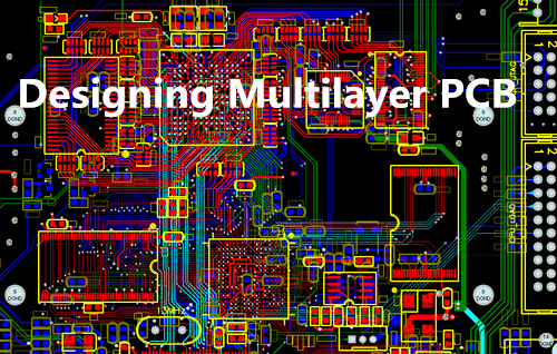
Cadence is a PCB layout and routing software that creates innovative circuit board designs. Its constraint-driven environment offers visual feedback and helps to ensure the manufacturability of PCBs. Cadence design software plays a crucial role in PCB industry. Regardless of the project complexities and sizes, this scalable software enables designers to meet all methodological technological demands for projects.
This design and layout creation platform enables schematic designers to achieve complex designs. Also, it offers enhanced features for PCB design. Cadence PCB design offer features that help you meet your unique design demands. Furthermore, this PCB designer offers real-time insights like advanced routing technologies, various design checks, and integrated analysis workflow.
Cadence offers innovative auto-interactive technologies that facilitate routing of high-speed interfaces. Also, Cadence streamlines the design process which helps engineers to ramp up high volume production.
Cadence PCB Design Tools

Cadence offers a lot of high-performance tool for your PCB design:
Miniaturization option
The miniaturization option helps to embed electronic components in the circuit board. Also, this option creates additional layers needed for the available embedded components and as well as check for the height of a component against layer stackup. Another crucial feature of this Option is that it handles design rules for HDI.
PCB layout solution
Cadence offers a scalable circuit board layout solution that allows users to run power and signal integrity checks in the circuit board tool. Furthermore, users can work in complex systems on a PCB layout. The flawless integration of RF, SI, and PI allows the greatest accuracy of virtual measurements.
Manufacturing option
Manufacturing option comprises three tools for output manufacturing. Also, documentation editor provides automatic documentation of assembly and manufacturing data. Furthermore, automation ensures a flow of documentation that result in consistent documentation.
Analog/ RF
As frequencies increase, the copper structures transform into electrical components as a result of their characteristic shape. The analog/RF option allows you to take these structures into account. Also, you can directly use the analog/RF option layout elements like filters or couplers in the schematic with normal schematic elements.
DFM Portal
Cadence PCB designer features a DFM technology that allows Allegro PCB or OrCAD PCB Editor users to verify manufacturability and reduce design cycles. Also, DFM rules can be checked in real-time while you design.
Team Design option
The team design option allows multiple people to work on a PCB layout. Also, this option can partition the design in different parts so that every user has his section. Another use of this option is that it allows users to simultaneously work together in a similar design database.
Benefits of Cadence PCB
Cadence offers a lot of benefits to users.
Powerful routing tools
Cadence features real-time, push/shove, any-angle routing which allows users to select from “hug-only” or “shove preferred modes. You can view real-time display of the amount of timing slack that remains for interconnect. Also, interactive routing allows interactive tuning of nets with delay constraints.
Constraint-driven design
Cadence PCB designer features a PCB editor which helps to create and edit simple and complex circuit boards. The PCB editor has a constraint-driven environment with extensive features that address various manufacturability challenges. Also, the constraint management system has spacing and physical rules. Every worksheet offers a spreadsheet interface that allows the users to manage, define, and verify the various rules in a hierarchical manner.
Furthermore, this application enables designers to make and review constraint that act as electronic blueprints. The constraint management system works with the PCB editor.
Front-end schematic capture and electronic design
Cadence PCB designer put analysis and simulation results at the fingertips of engineers. With this, engineers can make great decisions to meet reliability, cost, and time targets. Also, pre-route analysis and advanced simulation offer engineers the information they need to make high-performance designs. Power and signal integrity simulation help to drive design constraints.
Intuitive PCB editor
One of the benefits of using Cadence PCB design is its intuitive PCB editor. Also, this feature addresses various manufacturability and design challenges like etch creation, floorplanning, and placement. To achieve floorplanning, this PCB editor features placement replication for enhancing design placement.
Other benefits of Cadence PCB Design Software
- It allows layout engineers and schematic designer to work in parallel
- Comes with enhanced productivity features like the reuse of previous schematic designs
- Also, it assigns and manages high-speed design rules
- Gets rid of rework with powerful library management and creation
- Enables logical and physical design synchronization
- Also, it supports enterprise deployment and customizable user interface
- Allows multi-user parallel development
- The embedded constraint manager allows users to capture electrical and physical constraints
- Offers schematic and HDL design input
- It also offers interactive floorplanning and as well as component placement
- Reduces routing time for designs have high-speed interfaces
- Offers reliability verification in the layout tool
- It allows team collaboration
- Offers design partitioning for development teams that are dispersed
Frequently Asked Questions
How much is Cadence License?
Cadence license for a year for Virtuoso multi-mode simulation is $140,000. For Virtuoso Silicon Analysis and Virtuose XL, Cadence license costs $100,000 and $15,000 respectively.
Is Cadence similar to OrCAD?
OrCad is specially designed for schematic design. OrCad is a tool designed by Cadence. In 1999, Cadence design systems acquired OrCad and its product line.
Can I run Cadence on Windows?
Cadence can’t run on windows. This can only showcase its output on the windows machine.
What is the difference between Allegro and OrCad
Both Allegro and Orcad are design tools from Cadence. There isn’t much difference between these two. While Allegro is for PCB layout design, OrCad is for schematic design.
Conclusion
Cadence features powerful routing algorithms that can tackle complex and simple routes regardless of the density. Furthermore, Cadence is one of the most commonly used software for PCB design and layout.
