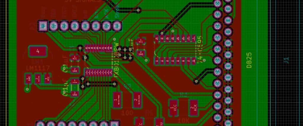
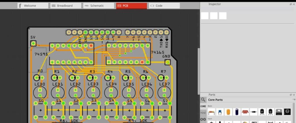
Altium Assembly Layer is a crucial component of the PCB design process. It is responsible for ensuring that all the components of a printed circuit board are accurately placed and connected. The assembly layer provides a visual representation of the board’s components and their respective positions, making it easier for manufacturers to assemble the board.
The Altium Assembly Layer is an essential tool for PCB designers. It enables them to create accurate and efficient designs, which can be easily manufactured. The layer provides a detailed view of the board’s components, including their dimensions, positions, and orientations. This information is used by manufacturers to assemble the board, ensuring that each component is correctly placed and connected. The layer also allows designers to check for any potential issues or errors before the board is manufactured, saving time and money in the process.
Overview
What is an Altium Assembly Layer?
An Altium assembly layer is a special layer used in PCB design software to indicate where components should be placed on a printed circuit board. The assembly layer is typically used to show the location of components, as well as any special instructions for assembly, such as orientation or polarity.
Why Use Altium Assembly Layers?
Using Altium assembly layers can help simplify the assembly process by providing clear instructions for component placement. This can help reduce errors during assembly, which can save time and money. Additionally, using assembly layers can help ensure that components are placed in the correct location and orientation, which can improve the overall reliability of the circuit board.
Altium assembly layers also allow designers to easily communicate important information to the assembly team, such as the location of test points or other critical components. This can help ensure that the assembly team has all the information they need to build the circuit board correctly.
In summary, Altium assembly layers are an important tool for PCB designers, providing clear instructions for component placement and helping to improve the reliability of the circuit board.
Creating Assembly Layers

Setting Up the Layer Stack
Before creating assembly layers in Altium, you need to set up the layer stack. The layer stack defines the order of the layers and their properties. To set up the layer stack, follow these steps:
- Open the PCB document in Altium.
- Go to the “Design” menu and select “Layer Stack Manager.”
- In the Layer Stack Manager, you can add, remove, and reorder layers. You can also define the properties of each layer, such as the layer type, thickness, and material.
- Make sure that the layer stack is set up correctly before creating assembly layers.
Defining the Layer Properties
Once the layer stack is set up, you can create assembly layers by defining their properties. Assembly layers are used to display the components and their placement on the PCB. To define the layer properties, follow these steps:
- Go to the “Design” menu and select “Layer Stack Manager.”
- In the Layer Stack Manager, click on the “Add Layer” button.
- In the “Add Layer” dialog box, select “Assembly” as the layer type.
- Define the properties of the assembly layer, such as the layer name, color, and transparency.
- Click “OK” to create the assembly layer.
You can create multiple assembly layers to display different aspects of the PCB assembly, such as the top and bottom components, silkscreen, and assembly notes. Make sure to define the properties of each layer correctly to avoid confusion during the assembly process.
In conclusion, creating assembly layers in Altium is a straightforward process that requires setting up the layer stack and defining the layer properties. By following these steps, you can create assembly layers that accurately display the components and their placement on the PCB.
Working with Assembly Layers
Placing Components
When working with assembly layers in Altium, it is important to start by placing your components correctly. The assembly layer is used to show the physical placement of components on the PCB, so it is essential that they are accurately placed. To do this, you can use the following techniques:
- Use the “Place Component” tool to add components to the assembly layer.
- Use the “Move” tool to adjust the position of components on the layer.
- Use the “Rotate” tool to change the orientation of components.
Routing Traces
Once your components are placed correctly, you can begin routing traces on the assembly layer. When routing traces, it is important to keep the following in mind:
- Use the “Route” tool to create traces on the assembly layer.
- Make sure that your traces do not overlap with any other components or traces on the layer.
- Use the “Via” tool to create vias as needed to connect traces between layers.
Checking Design Rules
Before finalizing your design, it is important to check your design rules to ensure that they are accurate and complete. To do this, you can use the following techniques:
- Use the “Design Rules Check” tool to check your design rules.
- Make sure that your design rules are consistent with your design requirements.
- Use the “Clearance Constraint” rule to ensure that there is sufficient clearance between components and traces on the assembly layer.
By following these best practices for working with assembly layers in Altium, you can ensure that your PCB design is accurate and complete.
Advanced Techniques

Using Blind and Buried Vias
Blind and buried vias are an essential technique for high-density printed circuit boards (PCBs). They allow designers to connect multiple layers without having to drill through the entire board. Blind vias connect an outer layer to an inner layer, while buried vias connect two internal layers. By using these types of vias, designers can reduce the size of the board and increase the number of layers.
Implementing HDI Technology
High-density interconnect (HDI) technology is a method of increasing the density of components on a PCB. HDI technology involves using microvias, blind vias, and buried vias to create a more compact design. By using HDI technology, designers can reduce the size of the board and increase its functionality. HDI technology is particularly useful for mobile devices, where space is at a premium.
Optimizing the Assembly Process
Optimizing the assembly process is an important part of PCB design. By optimizing the assembly process, designers can reduce the cost of manufacturing and improve the reliability of the board. One way to optimize the assembly process is to use surface mount technology (SMT) components. SMT components are smaller and lighter than through-hole components, making them easier to place on the board. Another way to optimize the assembly process is to use automated assembly equipment. Automated assembly equipment can place components quickly and accurately, reducing the time and cost of assembly.
In conclusion, by using advanced techniques such as blind and buried vias, HDI technology, and optimizing the assembly process, designers can create high-density PCBs that are smaller, more functional, and more reliable. These techniques require careful planning and execution, but when done correctly, they can result in significant benefits for the end product.
