PCB design software play a crucial role in PCB design. Altium PCB designer is one of the most popular PCB design software used in the PCB industry. Also, Altium is a sophisticated PCB design tool currently gaining popularity in the electronics industry. This PCB design software offers several features such as auto router and schematic.
Furthermore, this PCB design software features advanced tools that perform different circuit design tasks like circuit circulation and schematic. Also, the workspace in Altium designer can be specifically customized to meet your requirements.
What Does Altium Designer do?
Altium is a PCB design software that features several design tools. This software is in several versions as Altium keeps upgrading its features and adding more to it. Also, the most recent version of Altium is Altium Designer 20. This version is a result of several years of improvement and innovation. Furthermore, this version features integrated and advanced design tools. Therefore, it enables users to utilize all the features of the PCB design process efficiently.
Altium helps to perform PCB design, schematics, and more. Also, this PCB design software offers excellent control and ease of use. Its intuitive interface makes it very easy for users to integrate. Altium designer has helped several engineers to get creative and achieve good results with their creativity.
Altium workspace features two major components. The first component is the document editing environment which is at the right side of the software. Also, the Workspace Panels is the second component. These panels are on the left side of the software. Consumer electronics designers integrate Altium because of its simplicity and advanced features. This is because this software comes with sophisticated and advanced features.
How to Download and Install Altium Designer
In this section, we will go through how to use Altium Designer. This involves learning how to download and install Altium.
Download Altium Designer
Before you start downloading Altium designer software, ensure you sign up for the free user account. Visit Altium’s website to do this. After you have signed up, you can log into your account. Ensure you cross check the benefits and features of this PCB design software before you move to the next level. You can download this software after you have approved its benefits and components. Go to the download page to do this.
After the download has been completed, you can run the software on your PC by clicking on the Yes button. A page will display on your screen. Hit “Next” to continue. Also, you can now move to the Design Functionality where you can select your preferred functionality.
Install Altium Designer
After this, select the component folders to install your download. Then you will see a complete installation panel after some time. The time it takes for the complete installation panel to display depends on the speed of your internet. After installing the PCB design software, tick the box and click on “Finish” to close Altium.
Since you are running Altium Designer on your system for the first time, you will see a License Management Panel. Also, this Panel implies that the license you are using is invalid. Therefore, you will need to sign in to the account you initially created to have access to some valid permissions.
How to Set up Design Project in Altium Designer
The developers of Altium maintained that a project is a group of design templates required for PCB specification and manufacturing. For example, Multivibrator PCB is a project template that specifies all project-based settings.
Create a new PCB project
The first step to setting up a design project is to create a new circuit board project. Use the File section to design a new project. You can do this by choosing New Project and pressing the PCB Project button.
Include a schematic to the project
You will have to include a schematic sheet to your board project.
Set the document options
You need to set up the appropriate document options like Snap and sheet size before you start drawing the board.
Components and libraries
What you are adding to the PCB project will display as schematic symbols. Also, you can create components and place them from local libraries. You can also access components via the Content Vault.
Components assessment
Components assessment can happen through libraries window or explorer window.
Make libraries available
Altium allows the library components placement from existing libraries. In this case, it is necessary to install the libraries within the Available Libraries panel. You can access the dialog by simply hitting the Libraries tab.
How to Place Components on a Schematic
Components can be placed on any running schematic. Also, component assessment can happen in explorer window or libraries window.
Explorer window
Click on the component and select “Place.” After then, position the component and click press to insert. You can now appropriately position it and press to input. The Explorer wind will fade quickly once it floats on your workspace. This will allow you to have a view of the schematic drop components.
Also, you can click and get rid of parts from the Explorer window. Furthermore, hold the cursor down and ensure you release it. This will set the component.
Libraries window
You can asses and place components from the Libraries window by utilizing the Place tab. Also, the Place tab helps you to place the component. After, you have placed the component; you can leave the placement mode by right-clicking.
Multi-vibrator components
You can move to the Content Vault to view designators Q1, Q2, R4, R3, R2, R1, C2, C1, and P1. Place these designators to design a schematic.
How to Add Printed Circuit Board in Altium Designer
Wire the schematic
This is the first step when adding a board. You need to wire the PCB to allow connectivity between the various parts. Fortunately, this process is a very easy one.
Wiring guide
Left click to tie up the wire. After this, delete the initial anchor location by pressing backspace. Then clip the junction’s bearing by pressing spacebar. Hold the Spacebar and Shift at the same time to go through the wiring junction. You can exit the wire posting mode by right-clicking. Also, you can alternatively make use of the ESC tab.
After this, relocate the components by pressing CTRL, clicking and holding to move parts.
Net Labels and Nets
Net refers to the set of arts you connected. For example, a net can comprise C1, pin R1, and base Q1. Depending on the type of component pins, Altium designer software assigns each net to a label.
How to Create a New PCB

You will need to create a blank circuit board, label it and save before relocating a schematic design to a circuit editor. Before moving the schematic design, you will need to modify various settings of the bare board. These settings include resizing the shape of the circuit to the right size, defining the origin, and selecting the right snap grid. Also, you can click on PgDn and Ctrl to zoom and view the entire circuit.
Moving the schematic to the PCB editor
The best thing here is to directly transfer the schematic to the circuit board editor. With this, you don’t need to design another netlist document to speed up the transfer. Move to the circuit editor and click on Design. After this select Import Changes Multi-vibrator PrjPcb. Also, this will help you to compile the design and get some orders.
When the ECOs are successfully implemented, altium designer software will locate each impression in the Content Vault. Then it will place them in the PCB workspace.
Setting up the workspace
After completing the ECOs, you will see nets and parts display on the right side of the PCB workspace. You should change the PCB working area before you place the parts on the circuit board.
Configuring display layers
The PCB editor will also enhance some other non-electrical layers asides from the circuit board fabrication layers. Also, these layers are usually classified.
Output Documentation in Altium Designer
After you have completed the PCB layout and the design, you need to create output documentation. Output documentation is crucial in fabricating, assembling, and reviewing the PCB. Altium Designer has the capability to create different outputs for various purposes. There are three different categories of output in Altium.
Assembly output is the first category. This output features pick and place documents and assembly drawings. The documentation output is the second category. Also, this output comprises PCB 3D video, PCB prints, schematic prints, and PCB 3D prints. The fabrication output is the third category. This category consists of drill drawings, Gerber files, ODB ++, and IPC-2581 template.
Preparing several outputs
Altium designer integrates two different ways of configuring and creating outputs. These methods are individually or output Job template. The individual method involves keeping the configurations of every output in the Project template. Also, the through an output job template involves manually creating the outputs.
Gerber files configuration
PCB designers use Gerber to transfer data from PCB design to fabrication. Each Gerber document must correspond to a specific layer in the physical board. Also, if a board has holes, ensure you design the NC Drill template using similar measurements, onboard configurations, location, and resolution. Furthermore, the Gerber templates’ configuration can occur within the Gerber Setup panel.
BOM configuration
Altium Designer features an ActiveBOM that can help to configure the component data. Also, you can add additional non-PCB features.
BOM generation
You can generate a BOM output by visiting the Reports panel in the board editor and clicking the Materials Bill.
How to Map design data into the BOM
You must move the design data into an Excel BOM. Also, you can easily achieve this by inputting some special commands in the document used to create the BOM. You can use both Columns and Fields when creating the BOM file. Using the Columns and Fields will help to stipulate the right PCB layout. Also, Altium designer software comprises different files in the Templates section.
Benefits of Altium Designer
Altium Designer is a reliable PCB design software. Also, this software features everything that will help you design high-quality boards.
Cloud-based platform
Altium is a cloud-based PCB design platform that enables users to work from anywhere in the world. Also, anybody can have access to this software through the internet. Therefore, project team members can design and edit their works remotely.
Exceptional supply chain management
With Altium designer, you can design a BOM for your project. Also, Altium centralizes all manufacturing documents in a location. Therefore, this allows you to have quick access to these documents. Furthermore, this will help circuit designers to achieve success when designing electronic circuits.
Unified library management
The unified library management helps you to design your own boards without stress. Also, the library comprises a collection of models and components. Altium combines supply chain planning, schematic symbols and footprints in a location.
Interactive routing
Altium features a high-performance engine that helps you route your designs.
High density design
With Altium, you can design high-speed electronic circuits with ease. Also, the strong tuning engine offers support to advanced pattern features like Easy HDI structure integration.
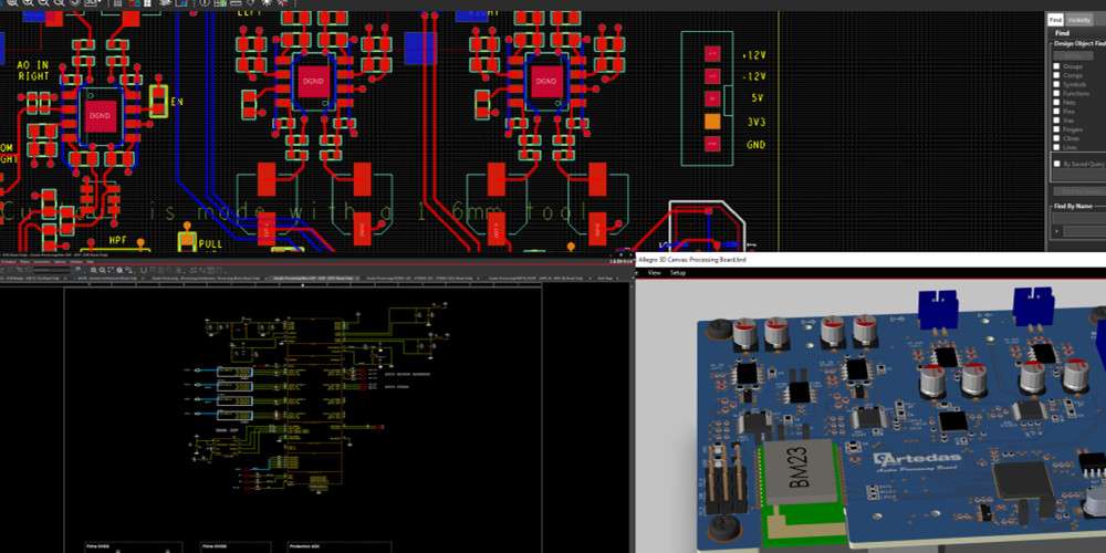
Native 3D PCB design
Altium enables users to create a 3D PCB design. Also, this newly integrated technology allows you to verify if your circuit will fit its final product enclosure. This helps to prevent any expensive redesigns. Also, 3D PCB views will verify your board designs and make any changes to them.
Other Benefits of Altium
- It can creates various PCBs
- Altium gives attention to micro details
- It is very compatible
- Also, it is user friendly
- The native 3D visualization helps users
- You can integrate all design resources in one location
- Also, it can combine multiple projects
- It can store data in the central point
- Also, it can convert files from other platforms
Conclusion
Altium designer is a go-to-PCB design software for PCB designers. PCB design is a process that involves making use of the right tools. Also, the type of software you integrate will determine the success of your project. Altium Designer features an intuitive and user-friendly interface. Furthermore, Altium Designer helps users to simplify the entire process. Altium has developed CircuitMaker, a PCB design application. Also, altium users have free access to these features.
