Protel PCB layout is an essential process in designing and manufacturing printed circuit boards (PCBs). PCBs are used in many electronic devices, from smartphones to computers, and are responsible for connecting and controlling the flow of electricity between components. Protel PCB layout involves designing the physical layout of the PCB, including the placement of components and the routing of electrical connections.
One of the key benefits of Protel PCB layout is its ability to optimize the performance and functionality of the PCB. By carefully designing the layout, engineers can ensure that the PCB operates efficiently and reliably, with minimal interference or noise. This is particularly important in high-speed or high-frequency applications, where even small variations in the layout can have a significant impact on performance.
Another advantage of Protel PCB layout is its ability to reduce manufacturing costs and improve time-to-market. By optimizing the layout, engineers can reduce the number of components required, simplify the routing of connections, and minimize the size and complexity of the PCB. This not only reduces the cost of materials and manufacturing, but also makes it easier to assemble and test the PCB, speeding up the development process.
What is Protel PCB Layout?
Overview
Protel PCB Layout is a software tool used for designing printed circuit boards (PCBs). It is a powerful tool that enables designers to create, edit, and manage PCB layout designs efficiently. The software was developed by Altium Limited, a leading provider of PCB design software and solutions.
Protel PCB Layout provides a user-friendly interface that allows designers to create schematics, PCB layouts, and bill of materials (BOMs) easily. The software supports a wide range of PCB design features, including:
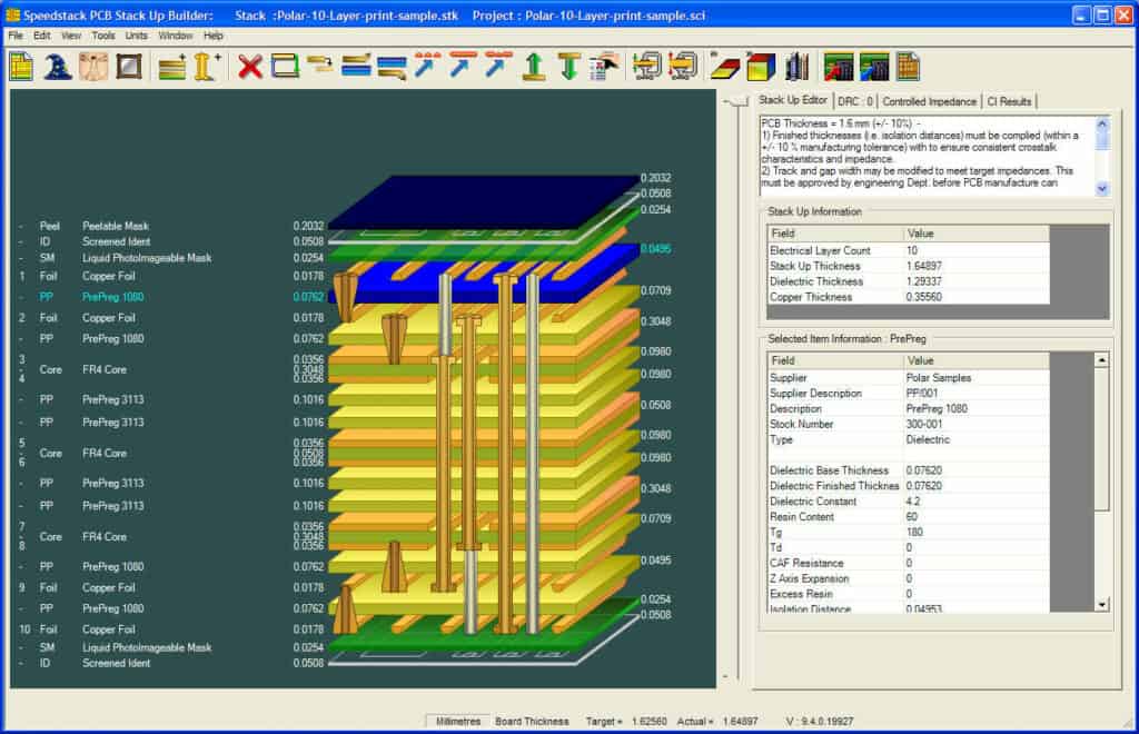
- Multi-layer PCB design
- Net connectivity and trace routing
- Component placement and management
- Design rule checking (DRC)
- 3D visualization and export
Features
Protel PCB Layout is designed to provide designers with a comprehensive set of features that enable them to create high-quality PCB designs quickly and efficiently. Some of the key features of Protel PCB Layout include:
- Advanced routing capabilities: The software provides advanced routing capabilities that enable designers to create complex PCB layouts with ease. It supports various routing modes, including manual, interactive, and automatic routing.
- Design rule checking: Protel PCB Layout includes an advanced design rule checking (DRC) system that ensures the design meets all the necessary requirements. The DRC system checks for errors such as short circuits, open circuits, and incorrect net connections.
- 3D visualization: The software provides a 3D visualization feature that allows designers to view their PCB designs in 3D. This feature enables designers to identify any potential issues with the design before finalizing it.
- Component management: Protel PCB Layout includes a comprehensive component management system that enables designers to manage their components easily. The software provides a library of pre-built components that can be used in the design process.
In conclusion, Protel PCB Layout is a powerful software tool that enables designers to create high-quality PCB designs quickly and efficiently. Its advanced features and user-friendly interface make it an ideal choice for both novice and experienced designers.
How to Use Protel PCB Layout?
Installation
To use Protel PCB Layout, you must first install the software on your computer. The installation process is straightforward and can be completed in a few simple steps. Once you have installed the software, you will be able to access all of the features and tools that it offers.
Designing PCB Layouts
Protel PCB Layout is a powerful tool for designing printed circuit boards (PCBs). To design a PCB layout in Protel, you will need to create a new project and add a schematic to it. Once you have created the schematic, you can begin laying out the components on the PCB. Protel offers a wide range of tools for designing PCB layouts, including automatic routing, design rule checking, and more.
Customizing Layouts
One of the great things about Protel PCB Layout is that it is highly customizable. You can customize the software to suit your specific needs and preferences. For example, you can customize the user interface, create custom libraries, and more. Protel also offers a range of plugins and add-ons that can be used to enhance the software’s functionality.
In conclusion, Protel PCB Layout is a powerful and versatile tool for designing printed circuit boards. With its wide range of features and tools, it is an excellent choice for both beginners and experienced PCB designers. By following the steps outlined above, you can get started with Protel PCB Layout and start designing your own PCB layouts today.
Tips for Using Protel PCB Layout

Best Practices
When using Protel PCB Layout, it is important to follow some best practices to ensure that your designs are accurate and efficient. Here are some tips:
- Start with a schematic: Before beginning your layout, create a schematic to ensure that your design is complete and accurate. This will save you time and effort in the long run.
- Organize your components: Keep your components organized by grouping them by function or type. This will make it easier to find and place components.
- Use design rules: Set up design rules for your project to ensure that your layout meets your specifications. This will help you catch errors before they become a problem.
- Optimize your layout: Optimize your layout by minimizing trace lengths and reducing the number of vias. This will help to reduce signal loss and improve signal integrity.
Common Mistakes to Avoid
There are also some common mistakes that designers make when using Protel PCB Layout. Here are a few to avoid:
- Not checking for errors: Always check your design for errors before sending it to production. This can save you time and money in the long run.
- Overcrowding your design: Overcrowding your design can lead to signal integrity issues and make it more difficult to troubleshoot problems.
- Not using design rules: Not using design rules can lead to errors and inconsistencies in your layout.
- Not optimizing your layout: Failing to optimize your layout can lead to signal loss and other issues.
By following these best practices and avoiding common mistakes, you can ensure that your designs are accurate, efficient, and of high quality.
Advantages of Using Protel PCB Layout
Efficiency
Protel PCB Layout provides a user-friendly interface that makes it easy to create and edit PCB designs. The software has a wide range of features that allow users to quickly and accurately design complex circuits. With Protel PCB Layout, users can easily create and modify PCB layouts, add components, and create custom footprints. This software also has an extensive library of pre-designed components, which saves users time and effort.
Accuracy
Protel PCB Layout uses advanced algorithms to ensure that PCB designs are accurate and error-free. The software has a built-in design rule checker that verifies the design against a set of predefined rules. This ensures that the design meets industry standards and reduces the risk of errors. Protel PCB Layout also has a 3D visualization tool that allows users to view their designs in real-time, which helps to identify potential issues before the PCB is manufactured.
Cost-Effectiveness
Protel PCB Layout is a cost-effective solution for designing and manufacturing PCBs. The software has a range of features that help to reduce manufacturing costs, such as the ability to optimize component placement and routing. Protel PCB Layout also has a built-in design for manufacturability (DFM) tool that ensures that the design is optimized for the manufacturing process. This helps to reduce the number of design iterations and ultimately saves time and money.
In summary, Protel PCB Layout is an efficient, accurate, and cost-effective solution for designing and manufacturing PCBs. Its user-friendly interface, advanced algorithms, and built-in tools make it an excellent choice for both novice and experienced users.
