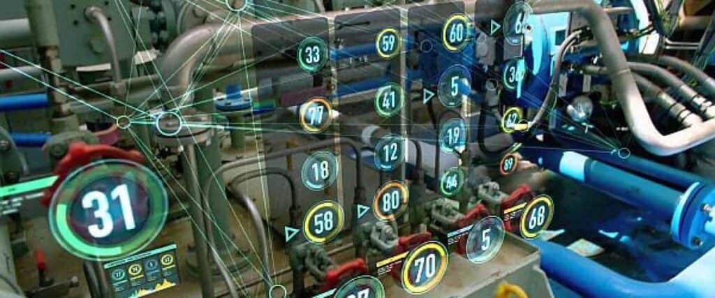
Manufacturing printed circuit boards (PCBs) is a crucial aspect of the Internet of Things (IoT) industry. PCBs are the foundation of most IoT devices, and their quality and reliability play a significant role in the overall performance of these devices. In recent years, the demand for IoT devices has skyrocketed, leading to an increased demand for high-quality PCBs.
Manufacturing PCBs for IoT devices requires a specialized set of skills and expertise. IoT devices are typically small, lightweight, and require low power consumption. As a result, the PCBs used in IoT devices are often smaller and more complex than those used in other electronic devices. Additionally, IoT devices are often used in harsh environments, such as extreme temperatures or high humidity, which requires PCBs to be designed and manufactured to withstand these conditions.
PCB Manufacturing Process
Designing the PCB
The first step in manufacturing a PCB is designing the circuit board. Designing a circuit board requires a computer-aided design (CAD) software that allows you to create a schematic of your circuit. You will need to have a thorough understanding of the circuit you want to create, as well as the components that you will be using.
Printing the PCB Design
Once you have designed your circuit board, you will need to print it. The most common way to print a PCB design is to use a laser printer. You will need to print your design onto a special type of paper called transfer paper. This paper is then used to transfer the design onto the copper layer of the PCB.
Etching the PCB
After printing the design onto the transfer paper, you will need to transfer the design onto the copper layer of the PCB. This is done by placing the transfer paper onto the copper layer and applying heat and pressure. Once the design has been transferred, the PCB is ready for etching.
Etching is the process of removing the copper that is not part of the circuit design. This is done by placing the PCB into an etching solution that dissolves the unwanted copper. Once the etching is complete, the remaining copper forms the circuit.
Drilling and Plating the PCB
After etching, the PCB is drilled to create holes for the components. The holes are then plated with a thin layer of copper to create a conductive surface for the components to be soldered onto.
Soldering the Components
The final step in manufacturing a PCB is soldering the components onto the board. This is done by placing the components onto the board and heating the solder to melt it and create a bond between the component and the board. Once all the components are soldered onto the board, the PCB is complete.
Overall, the PCB manufacturing process is a complex and precise process that requires a great deal of knowledge and skill. By following the steps outlined above, you can create high-quality PCBs that will meet the needs of your IoT project.
IoT Applications for PCBs
PCBs are an essential component of IoT devices. IoT devices require PCBs to connect sensors, actuators, and other components to the internet. PCBs are used in various IoT applications, including smart home devices, industrial automation, healthcare monitoring, and agricultural monitoring.
Smart Home Devices
Smart home devices are becoming increasingly popular as they provide convenience and efficiency. PCBs are used in smart home devices to connect sensors, control systems, and communication modules. Smart home devices can range from smart thermostats to smart locks, and PCBs are used in all of them.
Industrial Automation
PCBs are used in industrial automation to connect sensors, actuators, and controllers. Industrial automation systems are used to control and monitor various processes, including manufacturing, assembly, and testing. PCBs are used in industrial automation to improve efficiency, reduce downtime, and increase productivity.
Healthcare Monitoring
Healthcare monitoring devices are used to monitor vital signs, including heart rate, blood pressure, and oxygen levels. PCBs are used in healthcare monitoring devices to connect sensors, processing units, and communication modules. Healthcare monitoring devices are used in hospitals, clinics, and homes to monitor patients’ health.
Agricultural Monitoring
Agricultural monitoring devices are used to monitor soil moisture, temperature, and humidity. PCBs are used in agricultural monitoring devices to connect sensors, processing units, and communication modules. Agricultural monitoring devices are used in farms and greenhouses to improve crop yield and reduce water usage.
In conclusion, PCBs are an essential component of IoT devices used in various applications, including smart home devices, industrial automation, healthcare monitoring, and agricultural monitoring.
Challenges in Manufacturing PCBs for IoT

Manufacturing PCBs (Printed Circuit Boards) for IoT devices comes with its own set of challenges. In this section, we will discuss some of the major challenges faced by PCB manufacturers in the IoT industry.
Miniaturization of Components
One of the biggest challenges in manufacturing PCBs for IoT devices is the miniaturization of components. IoT devices are becoming smaller and smaller, and the components used in them need to be miniaturized to fit into the small form factor. This requires PCB manufacturers to use advanced manufacturing techniques to place the components accurately and precisely on the board. Miniaturization also means that the components are closer together, which can lead to interference and noise issues.
Power Management
IoT devices are often battery-powered, which means that power management is critical. PCB manufacturers need to design the board in such a way that it consumes as little power as possible while still providing the required functionality. This requires careful component selection, power supply design, and power management techniques.
Interference and Noise
IoT devices often operate in noisy environments, which can lead to interference and noise issues. PCB manufacturers need to design the board in such a way that it can withstand the noise and interference and still function properly. This requires careful layout design, component selection, and shielding techniques.
In summary, manufacturing PCBs for IoT devices comes with its own set of challenges, including miniaturization of components, power management, and interference and noise issues. PCB manufacturers need to use advanced manufacturing techniques and careful design to overcome these challenges and produce high-quality PCBs for IoT devices.
Future of PCB Manufacturing in IoT
The Internet of Things (IoT) is constantly expanding, and with it, the demand for PCBs is also increasing. The future of PCB manufacturing in IoT is promising, with several advancements and innovations in the field.
One of the most significant changes is the shift towards smaller and more compact PCBs. With the rise of wearable technology and smart devices, manufacturers are looking for ways to create smaller and more efficient PCBs. This trend is likely to continue in the future, as consumers demand more portable and convenient devices.
Another trend in PCB manufacturing is the use of flexible and rigid-flex PCBs. These PCBs can be bent and twisted, making them ideal for use in wearable technology and other applications where flexibility is important. As the demand for wearable technology continues to grow, the use of flexible and rigid-flex PCBs is likely to become more widespread.
Advancements in automation and artificial intelligence (AI) are also driving the future of PCB manufacturing in IoT. With the help of AI, manufacturers can optimize the manufacturing process, reduce errors, and improve quality control. This technology is likely to become more prevalent in the future, as manufacturers look for ways to increase efficiency and reduce costs.
Overall, the future of PCB manufacturing in IoT looks bright. With advancements in technology and a growing demand for IoT devices, manufacturers are likely to continue innovating and improving their processes. As a result, we can expect to see smaller, more efficient, and more flexible PCBs in the future.
