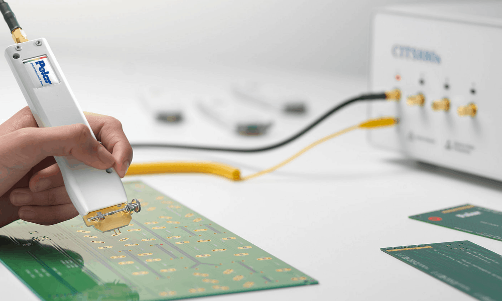
The high end electronic products are extensively manufactured in different parts of world in specialized PCB manufacturers and PCB assemblers. These products are high quality, high reliability and also expensive. This is because of the reason of using high speed and HDI (High Density Integrated) multi-layer PCBs inside these product. The PCBs are the core of any specialized high end commercial or military product like mother board, mobile phones, microwave telecommunication devices and other satellite control equipment or onboard electronic circuits. In this article we shall discuss about the “signal integrity” issues that are common to raise in high speed digital circuits PCBs and measures that a PCB designer takes by controlling the impedance of PCB to minimize signal integrity issues.
What is Signal Integrity?
The signal is basically the combination of voltage amplitude, the frequency and phase shift. In PCBs there are thousands of nodes or points which are interconnected with each other by means of “trace or track”. Signal integrity means that a signal when transmitted from one point on PCB to another point through transmission medium called trace is completed transferred to the receiver node by the transmitter node without any “signal reflection” or signal loss. However in practical cases this does not happen especially in high speed circuits. Because the transmission line is not properly terminated at the end node by a proper impedance equal to the “characteristic impedance” so the part of the signal transmitted is reflected back to the receiver hence generating signal vibrations and causing “signal distortion”. So we can say the mother of reasons of signal integrity issues is the “Impedance mismatch” at the transmitter and receiver ends on PCB trace i.e. transmission media.
Request Impedance PCB Quote, Pls send PCB file to Sales@raypcb.com Now
How to Control the Characteristic Impedance (Zo) and what it actually is:
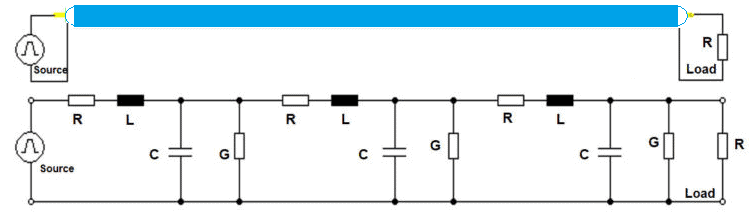
The characteristic impedance of the transmission line or trace is the combination of reactive and resistive components. The reactive components i.e. parasitic capacitance (C) and inductance (L) and resistive components i.e. resistance of transmission line (R) and conductance of transmission line (G). There are basically two types of transmission line (or trace for PCB). One is lossless where the components R and G are not present only reactive components make characteristic impedance and other is lossy where all four parts i.e. L, C, R and G make up the characteristic impedance. The below give is an example of a PCB trace showing its equivalent form in its reactive and resistive components
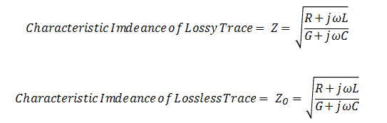
The mathematical formula for calculating characteristic impedance Zo for lossy and lossless traces is given below
Talking about the high speed multiplayer PCB, the most important factors that determine the characteristic impedance of a trace are
- 1- Trace width (W) and Thickness (T) also called trace geometry
- 2- The distance between signal image plane and signal layer (H)
- 3- Dielectric Constant of PCB base material
The trace itself is of two types.
- 1- Strip Line
- 2- Microstrip Line
The trace can be found on the external layers of PCB and can also be inside the internal layers of PCB as shown in the diagram below
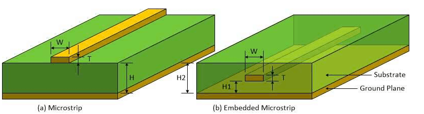
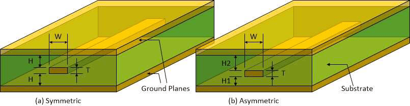
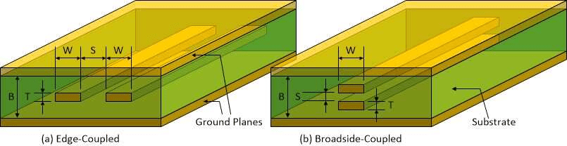
The Microstrip line or trace is the one that has ground or power plane only on one side of PCB. While the Strip line or trace is the one that has ground or power plane on top and bottomd both sides as shown in figure below.
The strip line is further classified as edge coupled and broadsided. As can be seen in figure below the distance between the two traces is denoted by “S”. This can be an example of differential line pair of LVDS (Low Voltage Differential Signaling)
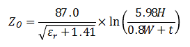
Microstrip Line Trace Characteristic Impedance Zo Calculation:
The equation to calculate the Microstrip transmission line or trace characteristic impedance according to IPC-2141 standards is give below
This formula is valid when![]() The propagation delay time of Microstrip trace is given by the formula
The propagation delay time of Microstrip trace is given by the formula
![]()
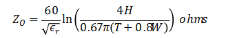
Stripline Line Trace Characteristic Impedance Zo Calculation:
Whereas the stripline trace characteristic impedance can be calculated according to the formula
This formula is valid when![]() The propagation delay time of Stripline trace is given by the formula
The propagation delay time of Stripline trace is given by the formula
![]()
Using these above formulas one can properly adjust the optimum characteristic impedance of the trace according to the requirement of application. Various standard protocols are mentioned below in the table with their respective characteristic impedances. The PCB designer must take care of these values to ensure signal integrity in PCB design.
| Standard | Impedance (Ω) | Tolerance |
| Ethernet Cat 5 | 100 | ±5% |
| USB | 90 | ±15% |
| HDMI | 95 | ±15% |
| IEEE 1394 | 108 | ±2% |
| VGA | 75 | ±5% |
| Display Port | 100 | ±20% |
| DVI | 95 | ±15% |
| PCIe | 85 | ±15% |
| Single Line LVDS | 50 | – |
| Differential Pair LVDS | 100 | – |
Request Impedance PCB Quote, Pls send PCB file to Sales@raypcb.com Now
How much speed is actually “HIGH Speed”..?
So what is exactly the high speed digital circuit is..? Well the answer is as precise as the question. The parameter that determines either the circuit is high speed or low speed is not the clock frequency which is mostly mistakenly discussed, but the “Rise Time tr” and “Fall Time tf” determines the circuit is high speed or not. According to the IPC standard, if the length of the signal’s rising or falling edge (also called Electrical Length) is greater than about one-sixth of the transmission line length then it is said to be “High Speed”. Look at the figure below.
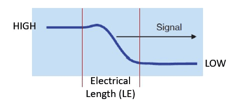
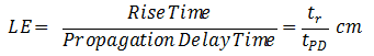
The mathematical representation of Electrical length (LE) is given by
Let the trace length is 100mm and rise time is 1.54nS and propagation delay time is 44pS, so we can calculate LE as
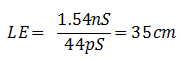
So the 1/6 of LE is 5.83 cm. So the 1/6th of LE is less than 100mm or 10 cm therefore the circuit is “High Speed” and techniques are need to be implemented to
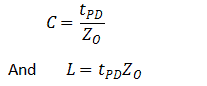
How to Estimate L and C values while Zo and tpd known:
In case when you know the characteristic impedance Zo and propagation delay time tpd then you can estimate the values of L and C of transmission medium i.e. trace by formulas below
Following methods must be adopted to ensure optimum signal integrity
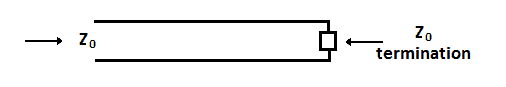
- 1- The transmission line must be terminated properly such that the load has the same equal impedance as of transmission line characteristic impedance Zo.
- 2- Ensure tight coupling of signal trace and reference (image) plane.
- 3- Tight coupling of power-ground planes. (enables high freq. decoupling)
- 4- Decoupling capacitors must be well implemented by placing them as close the Integrated Circuit pin as possible.
- 5- Low inductance power distribution.
- 6- Insert a reference plane or image plane for return current to avoid signal cross talk
- 7- Keep the via stubs length as short as possible or less than 15 mils because long via stubs can be a reason of signal reflection because they cause impedance discontinuity
- 8- The LVDS differential line / trace pair should be kept in length as short as possible
- 9- LVDS Traces line should be straight and traces should take 45Oangle turn instead of 90O
- 10- Try to minimize the number of Through holes
- 11- Distance between differential pairs should be kept more than 10 times so as to minimize crosstalk between lines. Ground through holes can be placed between differential pairs for isolation.
- 12- Distance between signal lines of differential pairs should be same
- 13- Both traces of differential pair must be on the same surface and must not be split across surface
- 14- Both traces of differential pairs must be on the same layer. Placing one trace on one layer and second trace on other layer can possibly lead to impedance mismatch due to PCB stacking misalignment during fabrication
- 15- TTL/CMOS signal traces and LVDS traces should be placed on different layers and isolated by ground/power planes.
