The new design methodologies and devices have impacted system companies. Also, new devices result in more challenges. New devices utilize the constantly evolving interfaces like DDR4, DDR3, Gen3, and more. Therefore, this calls for the need to learn new methods to implement them on the board.
Also, these increasingly complicated technologies drive companies to get their offerings to the market faster, with improved functionality. Therefore, several companies are now partnering or outsourcing with companies. As a result, PCB designers must find a solution that seeks to address their methodological and technological challenges.
What is Allegro PCB Designer?
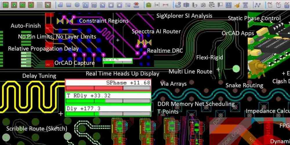
Allegro PCB design software is specifically designed for professional PCB and complete electronic systems development from Cadence Design Systems. This PCB design software features a powerful design environment that offers you exceptional PCB design experience. Furthermore, Allegro PCB designer features a scalable environment that addresses methodological and technological issues.
Allegro PCB designer comprises everything required to design a PCB layout with an extensive design flow. Furthermore, Allegro PCB designer features a constraint management solution, an auto-interactive router, and great interfaces for mechanical and manufacturing CAD. The PCB editor in Allegro offers a great routing and placement environment.
Also, Allegro PCB designers offer unparalleled performance. It completes your design with 64-bit performance. This software helps designers to detect and prevent field failures before they occur. As your design needs grow, Allegro adds advanced capabilities. Therefore, this eliminates any need to translate design files and learn new tools.
Benefits of Allegro PCB Designer
The Allegro PCB design software offers a lot of benefits to users. Therefore, it is highly preferred among PCB designers.
- The PCB design flow in Allegro gets rid of unnecessary iterations
- Comes with a constraint management system for creating, managing, and verifying constraints from front to back.
- Features a scalable PCB routing and editing platform in on-demand base with options for configuration.
- Includes a comprehensive rule set for design for assembly (DFA), high density interconnect (HDI), and design for fabrication (DFF).
PCB Editor Technology in Allegro
Allegro features a PCB editing environment that helps to edit and create simple to complex printed circuit boards. Also, this PCB editor comes with extensive feature that addresses various manufacturing and design challenges. This PCB editor features include:
Floorplanning and placement
The methodology of circuit board design solutions features a flexible and powerful set of placement capabilities. The PCB designer can assign subcircuits or components during floorplanning. A reference designator, part number, page number, and more can help to select and filter components. Precise management is crucial with today’s board comprising thousands of components.
Furthermore, real time assembly analysis can enhance this management by helping designers to improve efficiency and productivity by placing components based on EMS guidelines.
Constraint management
This system displays high-speed rules and physical spacing in real time. Constraint management is usually available at every stage of the design process. Also, each worksheet offers an interface that helps users to define and verify various rules in a hierarchical manner. The constraint management system is fully implemented with the PCB editor.
Interactive etch editing
This is a routing feature that offers interactive capabilities that provide controlled automation for user control management. Also, this feature maximizes routing productivity. Interactive routing allows interactive running of nets with delay constraints or high-speed length.
Placement replication
This is another feature offered by the PCB editor in Allegro. Placement replication enables users to route and place multiple similar PCBs in a design. Furthermore, it enables users to design a template by integrating one instance of routed and placed circuit board. You can use the already saved placement template with other designs. Designers can mirror or flip the circuit board from top to bottom layer when replicating placement.
The Manufacturing Option of Allegro PCB Designer

The Allegro PCB design software comprises a manufacturing option. This Manufacturing Option features a user-friendly suite of tools that makes streamlining the development of packages for products efficient. Also, the Manufacturing Option features three modules which are Panel editor, design for manufacturing, and documentation editor.
Panel editor
The panel editor module automates the process of panel documentation and definition. Thereby, it simplifies the design process. Also, this solution allows PCB designers to design electronic manufacturing documents that define the panel specification for successful assembly, inspection, and fabrication of their designs.
Documentation editor
This is a circuit board documentation-authoring tool that automates the process of documentation creation. Also, the documentation editor allows you to design the manufacturing drawings that drive PCB assembly and fabrication.
DFM checker
The DFM checker module is specially designed for designers and engineers that want to conduct manufacturing analysis in a robust environment. This module makes manufacturing analysis easy at any phase of PCB design process. Also, DFM checker provides extensive analysis for major PCB design tools, NC data, and Gerber files to ensure the content delivered to the manufacturers will reduce costly delays.
Allegro PCB Designer Miniaturization Option
The Miniaturization Option’s main feature is for components embedment into circuit boards. This Option is responsible for cutting out the necessary cavity which includes extra spacing. Also, the Miniaturization Option features the following:
Constraint-driven HDI design flow
Allegro users need to integrate a PCB technology with HAD due to the decrease in BGA pin pitches. Although miniaturization isn’t the main objective in several market segments, there is a need to develop a technology for fanning out a ball grid array.
Therefore, the Miniaturization Option provides HDI design flow with a set of design rules for various styles of HDI designs. Furthermore, this option consists of automation necessary for including HDI to reduce the time needed to create designs.
Embedded components
There are different ways designers can minimize end product size. One of these ways is to embed package components onto inner layers. Therefore, the Miniaturization Option provides the placement of embedded component. Also, it supports indirect and direct attach techniques and as well supports embedding components having dual-sided contacts. Furthermore, the Miniaturization Option helps to design and manage cavities on layers already defined for embedding components.
Conclusion
Allegro PCB designer helps designers with design for manufacturing (DFM) technology, high-speed design, and RF antenna. This software offers an exceptional design environment that provides you with the best PCB design experience.
