Majority of applications now work with wireless devices, which means that PCB antennas are in really high demand to ensure seamless communication. Consider simple devices such as wireless mice and emerging IoT and 5G networks. All these need wireless communication, and using a PCB antenna will play a huge role in developing them.
If your project deals with wireless connectivity, we will be looking closely at PCB antennas. These include the different types and ways in which we can design one. Now, let’s begin.
What Does a PCB Antenna Mean?
PCB antenna can be defined as a transducer that converts current to electromagnetic waves in any high frequency PCB. Furthermore, PCB antennas help in the conversion of high frequency current to EM waves, which propagates in the air.
In any high frequency PCB, there are two main PCB antennas. These are usually embedded into a PCB as an etched copper structure. In addition, one of the antennas serves as the transmitted signal of the radio frequency, while the other serves as the reflected receiver of the RF signal.
Also, the base materials of the circuit board help in transmitting the signals into the PCB antenna. High frequency circuits coupled with the PCB antennas make up the full high frequency PCB RF system.
In addition, as the PCB antenna size is designed so as to smaller and compact in size, in order to increase its efficiency, you can combine different microstrip patches so as to get the gain you deserve from the antenna’s minimized size. The patch size is dependent on the operating frequency’s wavelength of the target. The antenna length is also important.
Mostly, PCB antennas are semi-directional, directional, and omnidirectional antennas. The omnidirectional antenna has the ability to transmit signals in virtually all directions. However, the directional antenna features just one direction where you’ll need the signal. The semi directional type is usually specified with one angle where this signal propagates.
In order to fully understand the functioning of the PCB antennas, there is a need to understand what Impedance matching is as well as resonance circuits. To be able to get maximum efficiency, the load impedance and source impedance has to be equal.
Let’s continue by considering the types of PCB antenna.
What are the Different Antenna Types?
The high frequency PCB is usually created from antennas. Also, PCB antennas are usually embedded in it. To be able to have a good understanding of the different antenna types, we will discuss them one after the other.
Wire Antennas
The wire antenna is a cable, which extends higher than the printed circuit board (PCB) in a free space. This also gives the best performance and range as a result of its 3D dimensions and exposure.
PCB Antenna
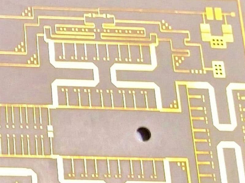
You can also call this the PCB trace antenna. This type of PCB antenna is simple just like the trace that is drawn on a printed circuit board. In contrast to wire antennas, this PCB antenna type is in 2D. This is because it lies just at the same place as the printed circuit board.
Chip Antenna
The chip antenna exists as a form-factor IC having a packed conductor in it. This compact size chip will offer a wireless range that is acceptable for BLE antenna designs.
Other antenna types include patch antennas and slot antennas.
What are the Antenna Parameters?
The following are the important performance antenna parameters
Return loss
This tells us how this antenna matches the transmission line of 50-Ω. Furthermore, the feature of the transmission line’s impedance is about 50 Ω. However, this could become different. However, the standard for commercial antennas and testing equipment is about 50 Ω.
Bandwidth
This helps in defining the operating frequency response of the antenna. This indicates the manner in which the antenna will match the transmission line across that specific board in question. For BLE applications, this is usually about 2.40 to 2.48 GHz.
Work with a wider bandwidth. This is because it helps in reducing the detuning effects that come as a result of the environmental changes that surrounds the antenna
Radiation Efficiency
Some of the non-reflected power transforms into thermal loss which then gets dissipated in form of heat. The reason for this loss is as a result of the conductor losses present in copper traces as well as the dielectric losses from the FR4 substrate. This dissipated heat helps in determining the radiation efficiency. Furthermore, 100% radiation efficiency means that all the non-reflected power becomes dissipated to free space.
Pattern of Radiation
The pattern of radiation reveals which of the directions experiences more radiation as well as the one that experiences less. The directional property plays a huge role in orienting the antenna in an optimal way to suit the application.
Majority of antennas have a direction where their RF frequency signals become more powerful. PCB antennas function similarly. They can also function effectively like a directional antenna.
Gain
In contrast to isotropic antennas, which radiate uniformly in all directions, the gain indicates the radiation from the desired direction. The dBi helps in expressing the gain by revealing the strength of the radiation field with respect to the appropriate isotropic antenna
Important Steps in PCB Antenna Design
Before you design the PCB trace antenna, you have to consider the factors below to ensure that the pcb antenna design is flawless.
Design Considerations
Pick the Best Antenna Type
Antenna designs come in different forms. The most common is the F type and meandering. This F type, which is the standard, features the best tradeoff between omnidirectional performance, size, antenna length, and efficiency. Also, the meandering traces are usually more compact, but they lag in their performance.
Consider the Construction of the PCB
The trace length of the copper PCB helps in determining the resonant frequency. Also, the higher this operating frequency is, then the shorter this trace will be. Every antenna requires an area surrounding the antenna trace having no copper traces or ground fill on a PCB layer (or the keep out area).
Furthermore, wide traces offer a wide bandwidth. You can cover it by making use of a gold flashed or solder mask. Finally, the electrical signal performance of the antenna is dependent on the substrate material, thickness and the dielectric constant.
The Ground Planes are Very Critical
There is a need for PCB antennas to have a ground plane because it makes them effective. The ground plane’s shape and size affects the impedance and performance of the antenna. Therefore, it ought to have a vias along the keep out area edge of the antenna.
Include the Matching Components
The mismatched antennas could bring a reduction in the range performance as well as the RF link budget. This is why a pi-network must be placed at the feed point of the antenna to prevent mismatch losses.
Impedance Matching
Asides from the components, make sure that the source and antenna impedance match (50 Ω) for the highest transfer of RF power. Do your best to ensure that the return loss is either equal to or less than -10dB.
Consider the Surrounding Environment of the Antenna
Metal enclosures, components, as well as other components could affect the tuning and the pattern of the radiation. Therefore, make sure that the antenna is kept away from metallic enclosures, metalized plastic and metal objects.
Tuning of the Design for some Applications
Lastly, make sure you tune the matching dimensions, for some applications. Furthermore, copying the existing designs isn’t right. This is due to the fact that the gain and radiation pattern changes as the parameters of the surrounding area changes.
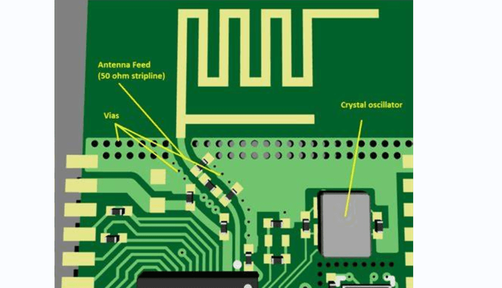
Antenna and Board Layouts
You should consider two sections on the printed circuit board. These include the crystal oscillator and the antenna sections. However, our focus will be on the antenna.
Design Steps
Once you are done placing the connectors and headers, fit the antenna trace and remember that it should have a trace impedance of 50Ω. This copper trace serves as the high frequency transmission line, while the impedance value relies heavily on the dielectric material and the board thickness.
Next is the trace width calculation. Using a 70 mils value for the trace width, 1.4 mils as the trace thickness, dielectric constant of about 4.5, and the dielectric thickness value of 39.3701, we will have a trace impedance value of 50.
Once the above calculations have been implemented, then the trace routing will be designed and then taken for manufacturing, programming, and then testing
What are the Types of Antenna Printed Circuit Boards?
- Wheels PCB antenna
- Yagi PCB antenna
- Log period PCB antenna
- Quadcopter antenna PCB
- Generic PCB antenna
- Flex antenna PCB
- UWB antenna PCB
- Patch arrays antenna PCB
- Custom antenna PCB
Summary
There you go! PCB antennas play a significant role in modern applications. The design above makes you build one for your projects easily. Make sure you stick to the design considerations. If there are any questions on your mind or you have some suggestions or comments, please reach out immediately.
