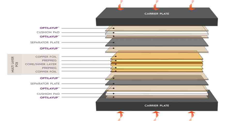
PCB design is an essential aspect of modern electronics. It involves the creation of a printed circuit board that connects various electronic components. The accuracy and efficiency of the PCB design process are critical to ensuring that the final product functions as intended.
One of the most important factors in PCB design is the accuracy of the design files. ATE PCB design, or Automated Test Equipment PCB design, is a process that uses automated testing to verify the accuracy of the design files. This process can help to identify and correct errors before the PCB is manufactured, saving time and money in the long run. ATE PCB design is becoming increasingly popular due to its ability to improve the accuracy and reliability of the final product.
Benefits of ATE PCB Design
ATE (Automated Test Equipment) PCB Design is a process of designing printed circuit boards that are used in automated testing. This method is gaining popularity among engineers and manufacturers due to its numerous benefits.
One of the most significant benefits of ATE PCB Design is its ability to reduce testing time. With the use of automated equipment, testing can be done faster and more efficiently. This not only saves time but also reduces costs associated with testing.
Another benefit of ATE PCB Design is its ability to improve the quality of testing. Automated testing equipment can perform tests with greater precision and accuracy than manual testing. This reduces the risk of errors and ensures that the product meets the required standards.
ATE PCB Design also allows for greater flexibility in testing. Automated testing equipment can be programmed to perform a wide range of tests, making it easier to test different types of products. This flexibility is essential for manufacturers who produce a variety of products.
In addition, ATE PCB Design can help reduce the need for human intervention in the testing process. This reduces the risk of human error and ensures that the testing process is consistent and reliable.
Overall, ATE PCB Design is a valuable tool for manufacturers and engineers who want to improve the efficiency and quality of their testing processes. With its ability to reduce testing time, improve testing quality, provide greater flexibility, and reduce the need for human intervention, ATE PCB Design is an excellent choice for any company looking to improve its testing processes.
Design Considerations for ATE PCBs
Designing a PCB for Automated Test Equipment (ATE) requires careful consideration of various factors. Here are some key design considerations to keep in mind:
Component Placement
When designing an ATE PCB, it is important to pay close attention to component placement. Placing components too close together can cause interference and lead to signal integrity issues. Additionally, components that generate heat should be placed away from sensitive components to prevent thermal damage.
Signal Integrity
Signal integrity is critical for ATE PCBs, as any signal loss or distortion can affect the accuracy of test results. To ensure good signal integrity, it is important to use high-quality materials and to carefully route traces to minimize noise and interference.
Power Integrity
Power integrity is also an important consideration for ATE PCBs. Power supply noise can affect the accuracy of test results, so it is important to use high-quality power supplies and to carefully route power traces to minimize noise.
Test Point Placement
Test points are used to connect the ATE to the PCB being tested. When designing an ATE PCB, it is important to carefully consider the placement of test points to ensure that they are easily accessible and that they do not interfere with other components or traces.
Test Coverage
Finally, it is important to consider test coverage when designing an ATE PCB. The ATE must be able to test all the necessary functions and features of the PCB being tested, so it is important to carefully plan the test strategy and to design the ATE PCB accordingly.
In summary, designing an ATE PCB requires careful consideration of component placement, signal integrity, power integrity, test point placement, and test coverage. By keeping these factors in mind, it is possible to design an ATE PCB that provides accurate and reliable test results.
Key Components for ATE PCB Design

When designing a PCB for automated test equipment (ATE), it is crucial to consider the components that will be used. The following are some key components that are essential for ATE PCB design:
Connectors
ATE PCBs require connectors to interface with the test equipment. These connectors must be able to handle high-speed signals and high pin counts. It is important to choose connectors that are reliable and easy to use. Some common connector types used in ATE PCB design include BNC, SMA, and SMB connectors.
Power Supplies
Power supplies are a critical component of any ATE PCB design. They must provide stable and accurate voltage and current levels to the DUT (device under test). It is important to choose power supplies that have low noise and high efficiency. Some popular power supply types used in ATE PCB design include linear and switching power supplies.
Test Points
Test points are used to access various nodes on the PCB during testing. They must be strategically placed to ensure easy access and accurate measurements. It is important to choose test points that are durable and have a low contact resistance. Some common test point types used in ATE PCB design include pogo pins and bed-of-nails fixtures.
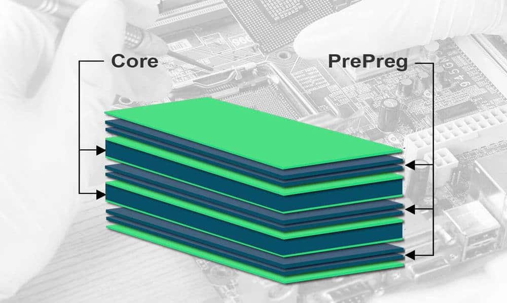
ICs and Passive Components
The choice of ICs (integrated circuits) and passive components (resistors, capacitors, inductors, etc.) can have a significant impact on the performance of the ATE PCB. It is important to choose components that are reliable, high-quality, and appropriate for the application. Some popular IC types used in ATE PCB design include op-amps, ADCs (analog-to-digital converters), and DACs (digital-to-analog converters).
In summary, when designing a PCB for automated test equipment, it is important to carefully consider the components that will be used. Connectors, power supplies, test points, and ICs/passive components are all critical to the performance of the ATE PCB. By choosing high-quality, reliable components, designers can ensure that their ATE PCBs will perform optimally and provide accurate test results.
Testing and Validation of ATE PCBs
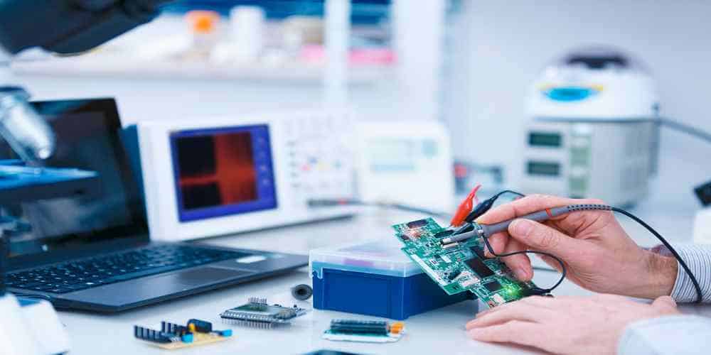
Testing and validation of ATE (Automatic Test Equipment) PCBs (Printed Circuit Boards) is a crucial step in the manufacturing process. It ensures that the PCBs meet the required specifications and perform as expected. The following are some of the methods used for testing and validating ATE PCBs.
Automated Optical Inspection (AOI)
Automated Optical Inspection (AOI) is a method used to inspect PCBs for defects such as short circuits, open circuits, and component placement errors. AOI machines use high-resolution cameras to capture images of the PCBs and compare them to the design files. This method is fast, accurate, and can detect defects that are difficult to detect manually.
In-Circuit Testing (ICT)
In-Circuit Testing (ICT) is a method used to test the functionality of individual components on the PCB. This method involves the use of a test fixture that connects to the PCB and applies electrical signals to the individual components. The results of the test are compared to the expected results to determine if the components are functioning correctly.
Functional Testing
Functional testing is a method used to test the overall functionality of the PCB. This method involves applying various input signals to the PCB and measuring the output signals. The results of the test are compared to the expected results to determine if the PCB is functioning correctly.
Environmental Testing
Environmental testing is a method used to test the durability of the PCB under various environmental conditions such as temperature, humidity, and vibration. This method is used to ensure that the PCB can withstand the conditions it will be exposed to during its lifetime.
In conclusion, testing and validation of ATE PCBs is a critical step in the manufacturing process. It ensures that the PCBs meet the required specifications and perform as expected. The methods used for testing and validation vary depending on the type of PCB and the requirements of the application.
Common Mistakes to Avoid in ATE PCB Design
Designing a PCB for Automated Test Equipment (ATE) can be a challenging task, even for experienced engineers. While there are many factors to consider, there are some common mistakes that can be avoided to ensure a successful design.
1. Inadequate Power and Ground Planes
One of the most common mistakes in ATE PCB design is not providing adequate power and ground planes. These planes are critical for providing a low impedance path for power and ground signals, reducing noise and improving signal integrity. Inadequate power and ground planes can lead to signal integrity issues, ground bounce, and other problems that can impact test results.
2. Poor Signal Routing
Another common mistake is poor signal routing. Signal routing can impact signal integrity and can result in crosstalk, reflections, and other issues that can affect test results. It is important to ensure that signal traces are routed properly and that they are kept away from noisy components and signals.
3. Inadequate Decoupling
Inadequate decoupling is another common mistake in ATE PCB design. Decoupling capacitors are used to provide a low impedance path for high-frequency signals and to reduce noise. Inadequate decoupling can lead to power supply noise, ground bounce, and other issues that can impact test results.
4. Incorrect Component Placement
Incorrect component placement can also be a problem in ATE PCB design. Components that are placed too close together can result in crosstalk and other signal integrity issues. It is important to ensure that components are placed in the correct locations and that they are spaced appropriately.
5. Lack of Test Points
Finally, a lack of test points is another common mistake in ATE PCB design. Test points are critical for debugging and troubleshooting and can help identify issues with the PCB design. It is important to ensure that there are sufficient test points on the PCB and that they are located in the correct locations.
In conclusion, designing a PCB for ATE requires careful consideration of many factors. By avoiding these common mistakes, engineers can ensure that their designs are successful and that they provide accurate and reliable test results.
