A thorough understanding of the Step by step process of Through-hole PCB assembly can help you make the most of your time and money. In addition, you will be able to understand how to apply the proper soldering techniques for various applications.
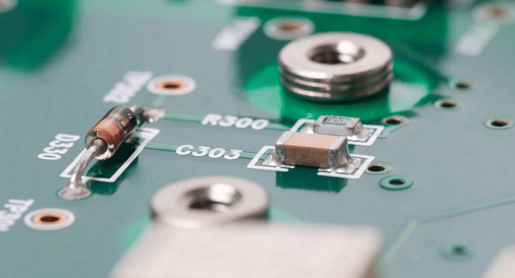
Solder paste stenciling
Printed circuit boards are an essential part of all types of electronics. With a market estimated to hit more than $50 billion by 2025, the PCB industry is poised to grow. Printed circuit board stencils help the PCB to achieve a better finish.
A stencil has an opening specially designed to deposit solder paste onto the PCB. Several PCB stencils include chemical etch stencils, laser cut stencils, and frameless stencils. These stencils consist of materials such as Mylar, polyimide, or paper.
The area ratio of a stencil is essential. This ratio indicates how much of the stencil’s open area helps to deposit solder paste. It also allows designers to calculate the approximate size of the hole PCB.
The Sn63/Pb37 alloy is commonly ideal as a screen printing material on PCB pads. Solder paste is a thixotropic material that changes from a solid block to a fluid when a runner is used to push it across the board.
Wave soldering vs. manual soldering
Whether manufacturing a through-hole PCB assembly or a single-sided PCB, choosing the right soldering method is essential. You don’t want to waste your time and money on a method that won’t produce results.
Selecting the right soldering method is a combination of several factors. You need to consider the board you are manufacturing, the type of components you are using, the size and number of boards you plan to produce, and the time you must devote to the process.
The correct soldering method choice will impact your through-hole assembly line’s production time and efficiency. You will also need to ensure that you keep the temperature at the right level. High temperatures can cause conductivity issues and cracks on the PCB. Therefore, it is essential to keep your through-hole assembly at a temperature above the melting point of the solder.
The correct wave soldering method will also depend on the type of components you are using. Selective soldering machines can also help protect specific components from heat damage.
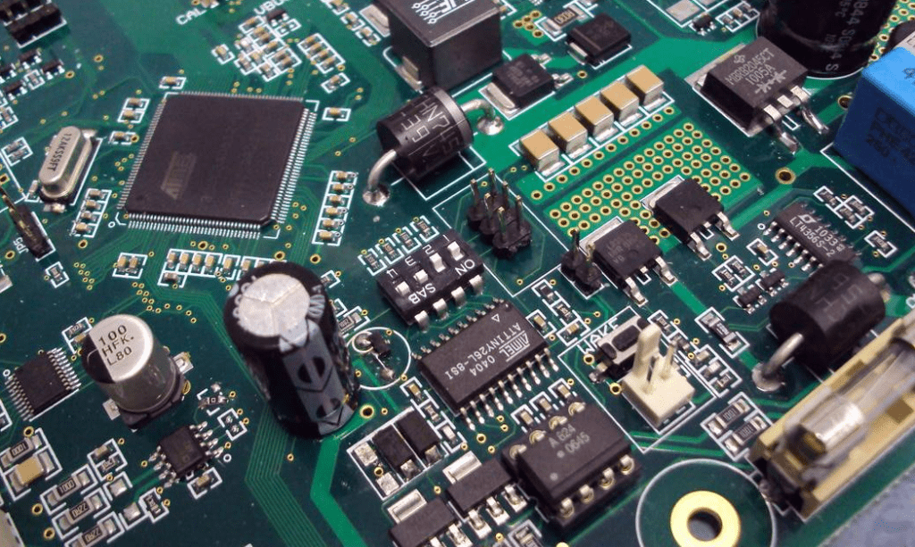
Inspection check and quality control
During through-hole assembly, a thorough inspection check is crucial to the overall quality of the product. It can reveal design flaws and manufacturing defects, ensuring a high-quality product.
The type of inspection check and quality control used will depend on the type of PCB and the components placed on it. For example, an X-ray inspection is typically helpful on more complicated PCBs. X-rays are non-invasive and provide high-quality imaging of the PCB internal quality.
Aside from X-rays, visual inspections also help to check PCBs. For example, an AOI (automatic optical inspection) program helps compare PCB photos to schematics. In addition, it can flag boards for technician inspection.
Another type of inspection is a manual inspection. We can do it with the naked eye or with a magnifying glass. It is also necessary to check for warpage and the thickness of the board.
PCB encapsulation
Whether you’re building a PCB or repairing one, it’s essential to follow a step-by-step process. The slightest error can impact performance and functionality. So ensure that your PCB meets all of your needs. PCBs are in almost every Electronic device.
Through-hole PCB assembly is a process that involves soldering leads through holes on a PCB. This provides a stronger physical connection and supports easy adjustments. Through-hole PCB assembly is beneficial for through-hole mounting bulkier components. It also adds to the power-handling capabilities of the board.
The through-hole assembly process is essential in defense applications and space applications. It’s still ideal for prototypes and testing.
Comparison Between Through-Hole PCB Assembly and Surface Mount Assembly

Whether you are a novice or a veteran in PCB assembly, you should know a few things about the difference between through-hole PCB assembly and surface mount assembly. These differences will help you to choose which one is best for your project.
Surface Mount Technology vs. Through Hole Technology
Choosing the best PCB assembly method is an important decision. Two common methods in modern electronics manufacturing are Surface Mount assembly and Through hole PCB assembly. Understanding the differences between these methods will help you select the best option for your needs.
Surface Mount, aka SMT, is a process that allows components to be soldered directly onto the surface of a PCB. This method is more efficient and allows smaller and faster boards. SMT is also more affordable. Surface mounting can be helpful for applications that require high-speed design, high-density circuits, and smaller sizes.
SMT can save you money because it doesn’t require drilling holes in your PCB. The process also allows through-hole mounting of components faster than Through Hole PCB assembly. However, there are still some downsides to surface mount assembly.
Through-hole PCB assembly has been the standard in the electronics industry for over 40 years, but it is not the only way to assemble PCBs. Aside from the surface mount and SMT, there are several other ways to assemble a PCB.
Surface Mount components occupy less space
Compared to Through-Hole PCB components, Surface Mount electronic parts are smaller and lighter. They also occupy less PCB surface space. As a result, they reduce the cost and weight of the PCB and the manufacturing process.
Through-Hole assembly has axial lead components inserted into drilled holes on the bare PCB. These through-hole component leads are then bent and shaped to fit the component. Compared to surface mount components, Through-Hole assembly is larger and requires more drilled holes.
Unlike Through-Hole components, SMT components go on both sides of the board. This is important in cases of high power consumption applications. Also, SMT assemblies are more resistant to vibration and impact. They are also cheaper and easier to assemble.
The through-hole technology was widely applicable before the emergence of SMT. However, compared to SMT, Through-Hole technology is more expensive and requires a lot of advanced manufacturing processes.
SMT components weigh as little as one-tenth of their conventional through-hole / thru-hole electronic components
During the last decade, a newer form of component packaging, called Surface Mount Technology, has become more popular in the electronics industry. This new style has many advantages, including reduced size and weight, improved shock resistance, reduced electromagnetic interference, and improved vibration resistance. However, despite these advantages, there are also some downsides.
Another advantage of this technology is its increased reliability. Since Surface mount devices use a reflow soldering process, they are less likely to break. This has led to a trend toward lead-free thru-hole assembly.
A second benefit is a reduced size and weight of axial lead components. These can be as small as one-tenth of their conventional through-hole / through-hole electronic components. They are also faster to place.
Solder-paste squeezer
Whether you are designing a PCB for a new project or looking to upgrade an existing PCB, you should consider whether you need a through-hole PCB or a surface mount PCB. There are several advantages to each type of PCB, and you should weigh them carefully before making a final decision.
First, it is essential to consider special electrical and thermal performance. You will also need to consider how much space your components will take up on your board. Typically, a through-hole component will require more space than a surface-mount component, and the board will need drilling for the axial leads.
Radial components are smaller and can be placed faster during thru-hole assembly. They are also less expensive than through-hole components. The lead spacing between the pins of a surface-mount component is usually 0.100 inches or more, while the lead spacing between a through-hole component’s leads is typically 0.1 inches or less.
Through-hole is more durable and gives a product a strong mechanical connection. It also allows for more power. But, you will need to make sure that you are getting the processing power you need within the footprint size of your PCB.
