Although there are many different types and sizes of electronics, circuit boards are used in practically all. Circuit boards remain essential in today’s computing because they offer a consistent, compact way to organize complex components in a limited space. The manufacture of PCBs will only increase as more and more gadgets, including those in the industry of electric vehicles, are outfitted with the computer chips.
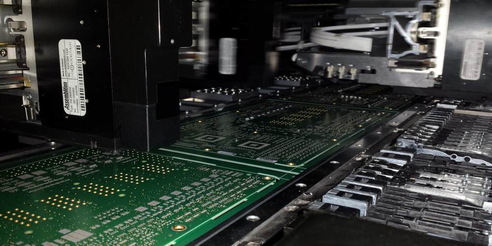
These components are becoming smaller as well as more complex as technology develops, necessitating the employment of the automated systems throughout their manufacturing process. Higher outputs of production, more sophisticated, cutting-edge components, and increased dependability as well as quality control are all made possible by factory automation during PCB manufacturing.
Furthermore, as a result of simulation technologies which can aid in the planning of Circuit board circuit layouts, the automated assemblies will just be becoming more effective.
In sectors searching for answers to their problems, PCBs serve as a helpful example of the capabilities offered by factory automation as a process that has completely embraced automation. On this, we will be discussing some ways automation technology is used in automated PCB manufacturing to speed up the production process.
Process Steps in Automated PCB Manufacturing
Although it is impossible to fully detail how each PCB manufacturer operates in this article, there are a few key components to the process of automated PCB manufacturing. Keep in mind that we will be thinking about making two-layer boards to keep things simple, but you can stack and bond more layers if you need to.
Additionally, despite the high level of automation used in this manufacturing process, workers are still required for jobs such as transporting the work-in-progress, setting up machines, and doing final inspections.
Drill Through and Via Holes
Drilling for the thru-hole components as well as vias is often the first stage in the process of PCB fabrication (followed by cleaning as well as deburring procedures). This is done with the drill machine that can create holes as small as 100 microns, or about the width of the human hair having a diameter of about 150 microns. Automatic bit changes are made for various diameters.
Layer Resist and Photo Plotting
Based on provided Gerber data, a negative picture of the completed copper gets printed on the transparent sheet to create PCB traces as well as fill areas of copper.
On the two sides of the panel, a photoresist photosensitive film layer is applied. The top as well as bottom of the panel are lined up with a printed sheet. UV lamps are used to harden this photoresist where there isn’t a printed image on that film. The copper beneath this unhardened photoresist is washed away after additional processing.
This board remains a part of the panel as a whole at this time, which could have a variety of designs. This cleaning is done frequently throughout the whole process of automated PCB manufacturing, and various inspections, particularly optical techniques, are done progressively to catch problems as soon as feasible.
Chemical processes and plating
In order to build up that original foil and provide a better and conductive channel to serve the vias as well as thru-hole connections, more copper is then electroplated to the PCBs. Customers can choose different copper plating thicknesses, and the entire process is meticulously managed to fit their needs.
HASL, Silk Screen, and Solder Mask
A liquid solder mask is placed to underlying two sides of your circuit board to protect your copper traces. These boards are then baked till they are semi-hardened after this has been done, and a printed sheet that is transparent is applied to the two sides. Similar to a prior photoresist procedure, this solder mask that is exposed gets hardened using a UV technique, and the uncovered solder mask would then be removed.
Next, a specific visible layer called the silkscreen is applied using the inkjet printer. This layer is utilized for identifying the component as well as other labeling purposes. Finally, to prevent uncovered solder pads against oxidizing, a procedure like HASL – hot air solder leveling is generally used. The PCB is then checked with the flying lead probe form of inspection to make sure it resists and conducts current flow way it is intended.
Routing and Profiling
A routing technique that is computer controlled removes the board’s profile as well as the internal features of the non-through hole after each Circuit board on the panel has been appropriately handled and examined. It is not necessary for these features and edges to become straight. Before this procedure, panels could be v-scored, or partially sliced in “v.” Customers can separate modules using V-scores, which are only allowed for straight lines.
Complete, pack, and ship
After thorough cleaning, additional processing to eliminate routing artifacts, and inspection, PCBs are ready to be packaged and delivered to consumers. This entire process has been great.
Benefits of Automated PCB Manufacturing

Throughout the entire process, components are loaded and positioned.
Not only are the components of the circuit board tiny, but they are also delicate. To prevent anything from breaking or being damaged during the manufacturing process, each piece must be handled carefully. Additionally, each component needs to be correctly aligned before each piece is carefully fitted in position. Eagle will incorporate multi-axis systems to offer the client parts to a bonding technology utilizing vision systems on the larger systems, such as wire bonding technology in EV industry.
Today robotic technology has specialized material handling abilities that can orient, lift, and position components precisely where they need to be for each stage of manufacturing.
Solder paste application
Soldering paste needs to be put to the proper portions of the circuit board before the components could be placed there. In order to do this, a stencil is placed upon that circuit board, after which the soldering paste is sprayed or rolled on the surface.
In addition, the automated application technologies can precisely manage the soldering applications’ direction and volume, preventing the waste of extra resources.
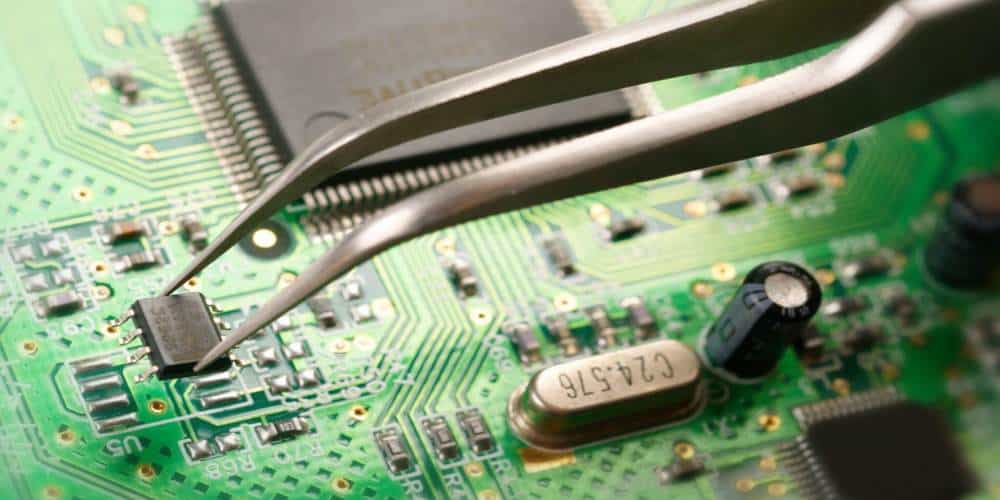
Automated component installation and wiring
The process of laying wiring and putting different computing components in place calls for the most accuracy. Because many of the components are so small and each printed circuit board needs a large number of them, putting them manually would become a tiresome task.
Automation, thankfully, comes to the rescue. Without the chance of human’s error, every circuit board could be put beneath a machine which is set up to apply the circuitry as well as other components.
Testing the functionality and wiring of circuit board
Testing circuit boards at the conclusion of assembly is crucial to ensuring the quality of the final product given the intricacy of the assembly process. In the initial phase, PCBs are examined to make sure that circuits are not misplaced and could otherwise impede a circuit board from delivering energy effectively.
Utilizing sophisticated software to confirm that the circuit board is operating properly is its second testing phase. Advanced testing abilities are necessary for these processes, and we build them into your assemblies as required.
Components miniaturization
As a PCB becomes smaller, it makes it possible to create ever-tinier components. Only with the manufacturing automation is this miniaturization possible. The most sophisticated automated systems available today are capable of applying lubricants and adhesives at microscopic scales, enabling assembly of correspondingly minuscule dimensions.
PCB tracing during the process of production
Factory automation is useful in the tracking of components as they travel down their production line in addition to assembling them.
In automatic product tracing, the component is given a bar code and perhaps other tracking devices, which is subsequently scanned at every checkpoint. Such tracking tags assist companies in keeping an eye on production rates, searching for process inefficiencies, and identifying any potential production faults.
PCB packaging
Lastly, with a large number of delicate goods, businesses must have the ability of carefully packaging them for distribution and transportation. Completed PCBs can be palletized, stacked, and wrapped using automated packaging to prevent damage while being transported.
There is less likelihood of human error
Circuitry assembly requires meticulous attention to detail. This becomes increasingly true as the products get smaller and their associated component sizes drop.
As a matter of fact, when human interaction is necessary, this may result in increased error rates. Since the process is now automated, accuracy is more likely. Automation expedites fabrication while simultaneously reducing costs. Additionally, it lessens the likelihood of errors.
Machines and people both make errors. However, while performing repetitive or delicate tasks, machines are far less likely to make mistakes. In certain circumstances, automated systems outperform human labor in terms of efficiency and dependability. In conclusion, using machines in exact settings can assist reduce the likelihood of error.
Marketing Time for the New Products Reduced
You may be sure that the boards you have ordered will arrive in excellent shape as well as move through several processes swiftly and effortlessly by outsourcing to any PCB assembly company that employs automated equipment. As a result, you won’t waste time or money.
Conclusion
Our objective is to provide you with circuit boards of the best caliber in the shortest amount of time. We continue to do this by enhancing our automation throughout the automated PCB manufacturing process.
