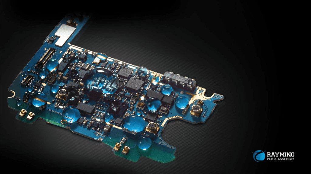
Manufacturing the printed circuit board (PCB manufacturing) involves a complex process. This starts with the product concept and finally ends with a completely functional PCB assembly. During the process a schematic is usually created that helps in capturing the general net connectivity, the ordering of the electronic components, and the laying out of the physical circuitry in the PCB design. After you have soldered the components on the board, coupled with completing the pcb assembly testing as well as verification, this circuit board becomes integrated in the whole system.
There are lots of intricate details that take the circuit board from the beginning to the end which has to be completed to ensure success. One of the areas that don’t usually get enough recognition is the bare board PCB fabrication. A PCB design usually gets so much attention as a result of the many software tools, which are useful in its creation.
Furthermore, PCB manufacturing process usually gets applauded in the completion of the end product. However, still lying somewhere is the process involved in circuit board fabrication. This is usually unknown outside the design world.
To reveal the origins of the bare circuit board as well as ways in which it is prepared to allow the assembling of the electronic components to it, we’ll be answering the simple question: What does the PCB fabrication process entail? In order to be properly acquainted, we’ll explain the necessary requirements for the construction of the top notch circuit board fabrication which a contract manufacturer can easily assemble.
What are the Basic Requirements for PCB Fabrication Process?
PCB fabrication process has to do with the building of the raw board which serves as the main foundation for the eventual printed circuit board assembly. Before the vendor can start with the building of the raw board, he or she must complete the checklist of the design details. Below are some important items to accomplish to start the PCB fabrication process. This also includes the data that these board vendors would be searching for.
Details of the circuit board
Before starting with printed circuit board layout (PCB layout), your design team has to work with the contract manufacturer so as to develop the configuration and the parameters of that physical board. Furthermore, the information is very important for the design layout. It also helps in deciding which of the vendors for your PCB fabrication is most appropriate for your job. Some of the details here include:
- Exposed copper balancing
- Via physical structure and types
- Considerations for printed circuit board panelization – PCB panelization
- Minimum trace spacing (exposed copper traces) and width
- Controlled impedance layers
- Board layer configuration and stackup
Finished PCB Design
To make sure there’s accuracy of PCB manufacturing, you have to complete the first and initial design. Even the update of the simple component which was not synchronized in-between the layout and the schematic can lead to changed footprint, which then results in a bad and faulty board build. Below are some of the design items that have to be checked off initially to ensure that the design is completed and then set for the PCB manufacturing process.
- Circuitry passes through a complete engineering review
- Layout and schematic databases are all synchronized and updated
- You have to place all the components on the circuit board, and the net connections are all routed.
- Completing the signal integrity, circuit simulation, and the power integrity analysis
- Checking the printed circuit board – PCB design rules as well as constraints and the errors are corrected
- Reviewing of the BOM (Bill of materials) for the available and current components
- Reviewing the DFM Design for manufacturing rules to ensure an error-free assembly
Full Data for the PCB Manufacturing Design
Now the design is set and the building is next. Here is the generation of some pcb assembly and fabrication data files, which are then presented to your contract manufacturer. Next, this PCB CM makes use of these files in conducting the reviews. Next is forwarding them to the hands of your fabrication vendor. He or she will give you the quote for building the raw boards. The data files must include:
- Gerber as well other formatted image files of the board layer
- The manufacturing drawings specially for the pcb assembly and fabrication
- BOM (Bill of materials)
- Locations of the component XY (pick & place)
- Locations of the test point
- Schematic
- Netlist
Having all these checklist items finished and set to go, your contract manufacturer will be able to go ahead with how to order the circuit boards that are necessary for assembly. Furthermore, your PCB contract manufacturer will have an already preferred list of fabricators. From this list, he will select that particular vendor having the capabilities that aligns best with the circuit board technical requirements.
Furthermore, another factor that is useful for choosing your fabrication vendor is if the board to be built will be a prototype or not. If this is the case, then your fabrication vendor should have the required capabilities that help in running your line of production outside the regular processes.
Also, they have to conduct the design reviews making use of the Gerber data that is supplied by your printed circuit board contract manufacturer. This helps in maintaining the best possible quality during the building of the prototype. Immediately you have selected your fabrication vendor, then you should go ahead with building the bare circuit board.
Explaining the PCB Fabrication Process
Having all the important and necessary data and design information with you, your PCB fabricator then starts building the bare board. You can fabricate so many circuit boards, which includes flex circuits, high density multilayer designs, and single-sided boards. Here, we will consider the important steps necessary for the fabrication of the multilayer circuit board.
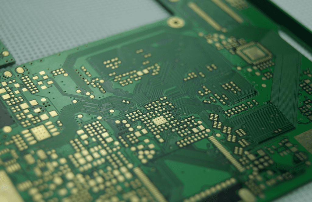
Creation of the Circuitry Images
Here, the initial step for circuit board fabrication is transferring the circuitry image data of your PCB from your manufacturing files which the CM has supplied to the board.
Furthermore, the data comes in a special file called Gerber. Though you can use other databases and formats. Using one of these two methods, you will transfer the image data to the board.
Direct imaging: The laser goes on to print the circuitry images on the circuit board directly. By doing so, it bypasses the importance of photo tools. It is more beneficial compared to making use of film due to its very precise nature, absence of alignment issues, and that photo tooling will not need any periodic recreation in replacing the worn-out films. Also, every layer must be laser printed, which makes the process a more expensive one.
Photo Tooling: This standard imaging process involved in the PCB fabrication process which has been used since the time circuit boards were mass-produced. The precision photoplotter helps in creating the circuitry images present on film that is useful in the whole fabrication process to serve as an important template for printing the images to the board.
The Circuit Board Layers
The multilayer circuit board is made up of different layers of metal conductors and dielectric material. Furthermore, it is made up of layer pairs having the dielectric core material involving glass fiber known commonly as FR4 and epoxy resin. This is sandwiched between both copper foil layers. Though there are several dielectric materials present, the FR-4 is known as the most commonly used core material for the PCB fabrication process.
The multilayer boards takes on the thinner version of a similar core structure that is used for creating the double sided board. Also, it laminates it altogether with the other structures in building the stackup of the board layer. Also, every layer has to be controlled strictly for its layer alignment, copper weight, and width to ensure a high-quality final product.
Inner Layer Circuitry Creation
The very first step for the PCB fabrication is the printing of the circuitry images to the inner layer cores:
- The core’s thin copper foil is covered using a photoresist material sheet.
- This photoresist is then exposed making use of either the UV (ultraviolet) light via direct imaging using a laser or photo tooling.
- Just the copper circuitry areas like copper traces and pads are exposed. This hardens or polymerizes the photoresist above the copper circuitry patterns. Also, this unexposed photoresist that is pliable is then removed chemically from copper.
- The core’s copper layers are then etched away. This leaves just those areas of the circuitry with protection from a polymerized photoresist.
- Also, this photoresist is then taken off leaving just the copper circuitry.
After completing this process, the core’s layers will undergo inspection via the Automated Optical Inspection (AOI system) for any defects. Immediately all the board’s inner layer pair has passed through the same process of automated optical inspection, then they are set for lamination in one full circuit board.
Lamination of the Layers Altogether
Altogether with the thin layers of the copper foil in covering the bottom and top sides external surfaces of the board, the layer pairs are then stacked to help in creating the PCB sandwich.
In facilitating the bonding of all the layers, every layer pair must have a “prepreg” sheet inserted in-between them. The prepreg is known as a fiberglass material that is impregnated using epoxy resin which melts during pressure and heat of the whole lamination process. Once the prepreg cools, it ends up bonding all layer pairs.
The composition of the board altogether all through this phase needs so much attention. Also, that individual must be detailed in order to maintain the right circuitry alignment on different layers.
After the completion of the stackup, the next is the lamination of the sandwiched layers. Also, the pressure and heat process fuses the layers altogether in one circuit board.
Drilling of Holes
Now, the next step for PCB fabrication has to do with drilling of holes into the board for the component mounting, non-plated holes, and thru-hole vias of different mechanical features. Furthermore, most thru-holes that are used in the circuit board are plated. Also, they are drilled 0.005 inches larger compared to the specified hole size that permits plating.
Furthermore, if this design has laser-drilled microvias or blind and buried vias, these are usually first fabricated before the board lamination. These additional process steps could bring extra costs to the board fabrication. However, they may be necessary for electrical performance and dense circuitry.
Immediately the drilling of the holes, they are cleaned making use of chemical and mechanical processes in removing debris and resin smears that appeared due to drilling. Also, the whole board’s exposed surface, which includes the holes’ interior, is coated chemically using a thin copper layer. This aids in creating a specific metallic base for the electroplating of additional copper in the holes as well on the surface.
Creation of the Bottom and Top Layer Circuitry
At this stage, the board is set to have the printing of the bottom and top circuitry images. In order to achieve this, this same photoresist is used with the inner layers. However, this time around, the circuitry will need no protection and then it has to be plated up using extra or additional copper.
- First, the inner layers, the bottom and top surfaces of the board are totally covered using a photoresist material. This includes the drilled holes that need plating.
- The exposure of the photoresist is by laser or UV. However, in contrast to all inner layers, the board’s surface layers are all exposed asides from the circuitry patterns.
- After the cleaning off of the unexposed photoresist chemically, the bare copper’s circuitry patterns are plated electrically with additional copper to help in building up the metal weight
- The next step is tin is then plated on all the whole copper circuitry. This is to serve as the protective later. Also, the photoresist is then stripped off from the remaining board to prepare for etching.
- Furthermore, is the etching of the board. This is to help in getting rid of all the copper asides from those metal circuitry areas that are well protected using the tin.
- Lastly, is the removal of the tin to leave the copper pads, thru-holes, and traces

Right now, the circuitry of the board has been finalized. However there are other steps to help complete the board fabrication
Silkscreen, Surface Finishes and Solder Mask
In order to protect your circuit board when assembly is ongoing, you apply the solder mask material making use of the process of UV exposure. This is very similar to what is used during the photoresist. The solder mask covers the whole board’s surface asides from the features and metal pads that have to be soldered.
Furthermore, aside from the solder mask, the component reference designators as well as other board markings will go on to be silk-screened on the board. Also, both the silkscreen and solder mask ink will get cured. This is possible through the baking of that circuit board in the oven.
Also, this circuit board will feature a surface finish that is applied onto the exposed metal surfaces.
With this, it will offer some protection to its exposed metal. Also, it assists the whole soldering operation all through the assembly. HASL (hot air solder leveling) is a very good example of a reliable surface finish.
First, this board is coated using flux. This helps in preparing it for the solder and it is then dipped in a molten solder bath. As this board is taken out from your solder bath, a blast of hot air helps in getting rid of excess solder mask present in the holes. Next, it smoothes all the solder mask present on that surface metal.
Inspection, Assembly Preparation and Testing
The final and last step of our PCB fabrication process is the preparation of the circuit board to be assembled. Also, if necessary, the circuit boards are all routed out of the manufacturing panels. In addition, the panels could be prepared for the breakout after the assembly. You can achieve this by routing out that board (for the small breakout tabs). Also, you can score the v-cut on the outline of the board.
Now, the completed product then passes through the continuity testing using automated test equipment like the flying probe test. Also, tests usually search for unintentional shorts present between the nets which would have invalidated the board. Immediately the testing has been completed, and the board has been able to pass inspections, it is then shipped to the contract manufacturer to start with the component assembly.
Features to Consider Before Choosing a Company for Your PCB Fabrication
Manufacturing high quality printed circuit boards needs a great partnership with the PCB contract manufacturer as well as a PCB fabrication vendor that will be chosen to handle the bare boards. To make sure you get the expected PCB fabrication quality, there are some attributes to check for. These include:
- ISO 9001 certification
- Has experience in that PCB technology required
- It can verify the specific design
- They are cost competitive and deliver quickly.
Conclusion
The printed circuit board – PCB fabrication process could be a simple and direct one. However, there are some things to put in place before you begin. Also, to ensure top quality printed circuit boards, you must consider some features before working with a PCB fabrication company.
