Buried Via PCBs are an advanced type of printed circuit boards that allow for higher component density and improved signal integrity. They are a vital innovation in modern electronics, especially for complex designs that require high performance and precision. In this article, we’ll dive into the fundamental aspects of Buried Via PCBs and discuss how they differ from traditional through-hole and microvia technologies.
At the core of any Buried Via PCB is its unique via structure. As the name suggests, these vias are completely hidden within the internal layers of the board, enabling electrical connections between different layers without taking up valuable surface space. This not only maximizes the board real estate but also minimizes signal interference and cross-talk, which can degrade the overall performance of the system.
The fabrication process of Buried Via PCBs involves specialized techniques and equipment, ensuring high reliability and consistency. The choice of materials, lamination process, and drilling technologies all play a critical role in the overall performance and integrity of the final product. With this understanding, engineers, designers, and manufacturers can leverage Buried Via PCB technology to create cutting-edge electronic devices that meet stringent requirements and push the boundaries of what is possible.
Understanding Buried Via PCB
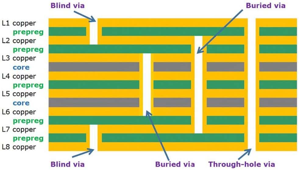
Types of Vias
There are primarily three types of vias used in PCBs:
- Through-hole vias: These vias pass through the entire PCB, connecting layers on both sides of the board.
- Blind vias: These vias connect an outer layer to one or more inner layers but do not go through the entire board.
- Buried vias: These vias connect two or more inner layers without reaching the outer layers of the PCB.
Definition of Buried Via
A buried via is a type of via that connects two or more inner layers of a printed circuit board (PCB) without having any connection to the outer layers. This type of via is typically used to save space on the PCB and to maintain signal integrity, especially for high-speed and high-density applications.
Buried vias are created during the lamination process of a multilayer PCB. Individual layers are first stacked, followed by drilling and plating the vias on these layers. Next, the layers are pressed together to form a complete PCB, and the vias become fully buried within the structure.
The use of buried vias can provide several benefits, such as:
- Increased board density: By removing the need for pads and traces on the outer layers, buried vias can help achieve higher component density on the PCB.
- Improved signal integrity: Since buried vias are shielded by the outer layers, they can help reduce electromagnetic interference (EMI) and maintain signal integrity.
- Reduced board size: With more available space on the outer layers, the overall size of the PCB can be reduced.
However, the use of buried vias can also result in some challenges:
- Increased manufacturing complexity: The fabrication process for multilayer PCBs with buried vias can be more complicated and time-consuming, resulting in higher costs.
- Limited repairability: Since buried vias are not accessible from the outer layers, troubleshooting and repairing a PCB with buried vias might be more difficult.
Despite these challenges, buried via PCBs can be a viable option for designers when the benefits outweigh the potential drawbacks.
Applications of Buried Via PCB
High-Density Interconnects
Buried via PCBs are widely used in high-density interconnect (HDI) applications due to their ability to reduce the size of a PCB, save space, and improve functionality. HDI PCBs require a greater number of connections in smaller areas, making buried vias an ideal solution for achieving compact designs. Some examples of HDI applications include smartphones, tablets, and laptops.
Telecommunications Equipment
In telecommunications equipment, signal integrity and high-speed performance are crucial. Buried via PCBs provide a conducive environment for these requirements, as they can effectively minimize Signal reflection, reduce interference, and enhance signal routing, making them well-suited for telecommunications systems such as routers, switches, and base stations.
Medical Devices
Medical devices often demand high reliability and precision. Buried via PCBs help meet these requirements by enabling more complex routing, improving electrical performance, and increasing component density. Medical devices that benefit from buried via PCBs include pacemakers, defibrillators, and diagnostic imaging equipment.
Manufacturing Process and Techniques

Drilling Buried Vias
Buried vias are created during the drilling process, which involves the use of specialized drilling machines to create precise holes in the PCB substrate. These holes connect the internal layers of the PCB without extending to the outer layers. During this process, the location and depth of the holes must be carefully planned and monitored to ensure accurate connections between the specified layers.
Layer Lamination and Bonding
Once the buried vias are drilled, the PCB undergoes a layer lamination and bonding process. This process entails stacking the layers of the PCB together and using heat and pressure to bond them. Each layer must be precisely aligned to ensure connectivity between the buried vias and the corresponding layers of the circuit board.
Copper Plating
After the lamination and bonding process, copper plating is performed to interconnect the buried vias by filling them with copper. The copper plating process usually consists of a series of electrochemical deposition steps, where a thin layer of copper is deposited on the surface of the vias. This process ensures a strong electrical connection between the conductive layers.
In summary, manufacturing a buried via PCB necessitates meticulous planning and execution, paying close attention to the drilling process, layer lamination, bonding, and copper plating. By following these steps, a high-quality, reliable, and efficient PCB with buried vias can be produced.
Advantages and Limitations
Size and Space Efficiency
Buried Via PCBs offer significant size and space efficiency in comparison to traditional through-hole PCBs. With buried vias, designers can connect internal layers without extending vias through the entire board. This allows for more compact designs and better utilization of board space, especially for high-density interconnect (HDI) applications. Furthermore, it permits additional routing channels, improving signal integrity and reducing electromagnetic interference (EMI).
Cost Implications
While the use of buried vias helps improve compactness and signal performance, they also come with certain cost implications. The manufacturing process for buried via PCBs is more complex and time-consuming than traditional through-hole PCBs, which can lead to increased production costs. However, for applications requiring high-density interconnects or advanced thermal management, the benefits offered by buried vias offset the increased costs.
Thermal Management
Buried vias can significantly improve thermal management in a PCB design. By providing shorter paths for heat dissipation compared to traditional through-hole vias, they help to reduce hotspots and prevent temperature-related issues. Additionally, buried vias can be placed strategically throughout the design to enhance heat dissipation paths and maintain thermal stability.
