A programmable circuit board (PCB) is a digital circuit board that can be reconfigured. It is an electronic device whose ability to be reconfigured is due to the electronic components that it comprises.
The two main components of a PCB are; a logic device, and a digital circuit board, harnessed and fused according to computer architecture. Although the interconnectivity and fusion of the PLD and circuit board make up the essential PCB, these three devices are yet different from one another as stand-alone devices.
Computer architecture as described here is simply a subcategory of computer engineering that defines the function and implementation of a computer system based on a fixed set of rules and methods.
This branch of computer engineering looks at the structure of the individual components of a computer, in this case, the programmable logic device and digital circuit, and considers the interconnectedness.
The branch that specifically deals with devices like this is reconfigurable computing. This device has software and hardware components working hand in hand. Here’s a look at the individual components of this device and how they work together.
What’s on the Board?
A digital circuit board
This is the foundation on which a PCB is built. This digital circuit board is a printed circuit board that operates a digital electronic circuit. Before proceeding let’s define these terms.
Printed circuit board
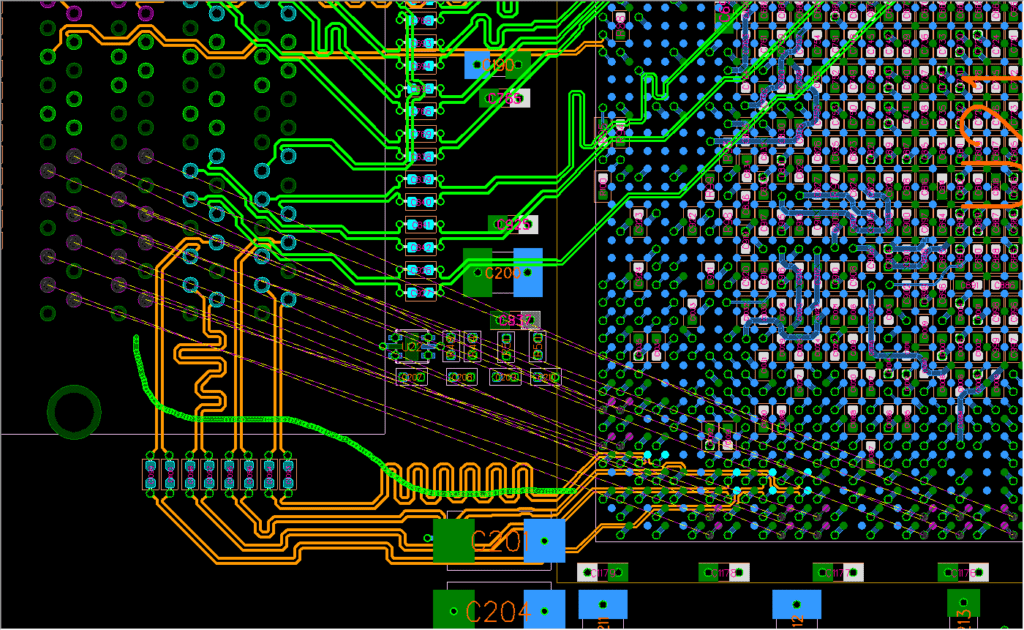
A printed circuit or printed wiring board is a connection method used in electrical engineering to safely link parts of electronics together. It has conductive and insulating layers arranged in a laminated arrangement.
Each of the conductive layers is constructed with a pattern of traces, planes, and other features that are etched from one or more copper sheet layers laminated onto or between sheet layers of a non-conductive substrate. These features resemble the pattern of wires on a flat surface.
Electrical components are attached to this board through conductive pads on the outer layers of the board. Typically these conductive pads are designed to be in the shape of the terminals of the electrical component. Because this board is used in almost every electrical device these days, manufacture is much higher now than it has ever been, howbeit automated.
To manually produce this board per unit will take an insane amount of extra effort because individuals would need to be very particular in the layout of the circuit. To avoid a waste of human effort and to ascertain a homogenous standard, printed circuit boards are produced through a process called electronic design automation.
Electronic design automation
It is a process based on a set of software tools that create electronic systems like integrated circuits and printed circuit boards. Chip designers use these tools to design and assess semiconductor chips.
This automation process greatly reduces the risk of error that may come from manual design, seeing as some modern chips can have up to a billion microcomponents functioning as one. There are five major stages that these software tools focus on in the design flow.
- Design: there are some variations including high-level synthesis, logic synthesis, schematic capture, and layout.
- Simulation: there are different levels at which simulation is accurate. They include transistor simulation which is accurate at the device level, a Logic simulation which is accurate at the boolean level, and a behavioral simulation which is accurate at the interface level. There also includes hardware emulation, technology CAD, and Electromagnetic field solvers.
- Analysis and verification: This stage includes functional verification, clock domain crossing verification, formal verification and model checking, equivalence checking, static timing analysis, and physical verification
- Manufacturing preparation: this stage involves mask data preparation, chip finishing, producing a reticle layout, layout-to-mask preparation, mask generation, automatic test pattern generation, and built-in self-test.
- Functional safety: this stage involves functional safety analysis, functional safety synthesis, and functional safety verification.
Digital Electronic Circuits and Logic Gates
Large groups of logic gates are frequently packed together in an integrated circuit to create digital electrical circuits. A logic gate is an electronic device that performs a Boolean function, which is a logical operation on one or more binary inputs that results in a single binary output.
Although vacuum tubes, electromagnetic relays (relay logic), fluidic logic, pneumatic logic, optics, molecules, or even mechanical components can be used to build logic gates, diodes and transistors are the most common electronic switches used to produce logic gates. MOSFETs (metal–oxide–semiconductor field-effect transistors) are now used to make the majority of logic gates.
It is possible to develop a physical model of all of the Boolean logic, and thus all of the algorithms and mathematics that can be described using Boolean logic. Logic gates can be coupled in the same manner that Boolean functions can be combined.
Here’s how. In Boolean logic, the values of the variables are truth values true and false, which are mathematically represented as 1 and 0 respectively. The major operations of Boolean algebra are the conjunction (and), the disjunction (or), and the negation (not), denoted by certain mathematical signs.
This is in contrast to elementary algebra, where the variables’ values are numbers and the prime operations are addition and multiplication. Because of this, Boolean algebra is suitable for describing logical operations, just as elementary algebra is suitable for describing numerical operations.
Programmable Logic Device
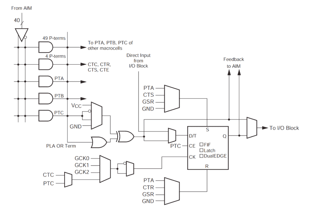
A programmable logic device is a device that is manufactured with an undefined function, and for it to be used in a circuit, the device has to be programmed to carry out the desired function.
It is worthy of note that programming this device for a specific function changes the connections between gates inside the PLD. When designing complex logic functions, the whole process is less complicated and simpler with the use of a programmable logic device as opposed to a fixed logic device.
Instead of thinking hard about how to configure fixed logic devices to appropriately work in, and serve the complex function, PLDs can be used in any configuration according to the design, as long as they’re programmed accordingly to suit the complex logic.
PLDs are basically of two types; simple programmable logic devices also known as SPLDs, and complex programmable logic devices also known as CPLDs. PLDs are programmed by PLD programming languages.
PLD Programming Languages
This is the language that logic compilers known as PLD programming devices use as source code. The language is known as Hardware description language and there are a few variants. For simple devices, HDLs like PALASM, ABEL, and CUPL are regularly used, but for more complex devices, HDLs like Verilog and VHDL are used.
The HDLs are similar to the various types of programming languages. The difference is that, unlike how programming languages configure a piece of software and set the rules of its function, hardware description languages configure and set the rules of function and behavior of circuits in electronics.
PLD Programming Devices
PLD programming devices or device programmers, like software compilers, are logic compilers for a specific type of hardware (PLDs). They deliver the boolean logic pattern into the programmable device by detecting and deciphering HDL source code and interpreting that into hardware functionality for the PLD.
In times past PLD manufacturers produced their device programmers for their set of logic devices, but these days have seen universal device programmers come up with the ability to function with differing sets of logic devices from different manufacturers. PLDs, although programmable, can retain their configuration once programmed due to their constituents. PLDs consist of a logic device and a memory device.
It is this memory device constituent that allows PLDs to retain their configuration. The memory device does this by storing the pattern that the chip receives during programming. Most of the ways that data can be stored have already been incorporated into PLDs as created over the years.
Some of these methods are:
- Silicon antifuses: These connections are created inside the device by passing a voltage over a modified region of silicon. They are known as antifuses because they operate in opposition to standard fuses, which start as connections before being disrupted by an electric current.
- S-RAM: This memory type is volatile, which means that if the power is turned off, its contents are gone. SRAM-based PLDs must be programmed each time the circuit is turned on as a result. Usually, another component in the circuit completes this automatically.
- Flash memory: because it is non-volatile, this sort of memory keeps its data even when the power is turned off. Storage happens in memory cells (floating-gate MOSFETs) and is erasable and reprogrammable as needed. This makes it practical for PLDs that might be constantly reprogrammed, such as prototype PLDs. Similar to EPROM, flash memory is a type of EEPROM that stores data utilizing trapped electric charges. As a result, Flash memory can store data for many years, though not for as many years as EPROM.
- EPROM or EEPROM: This memory cell is a metal-oxide-semiconductor field-effect transistor (MOSFET), or MOS transistor, which may be turned on by trapping an electric charge on its gate electrode. A PAL programmer does this task. The chip must be subjected to intense UV light in an EPROM eraser to remove the charge, which lasts for many years.
What Does It Do?
A real-life application of a PCB is in the manufacture of human interactive devices (HIDs). These devices are also known as human interface devices. They are computer devices that take input from a human source and deliver output back to the human.
There are many common examples of HIDs. Devices like computer monitors, loudspeakers, headsets, keyboards, webcams, fingerprint sensors, mice, and touchpads, are all common examples. There are less common examples like drive simulators and flight simulators, and dance pads.
Perhaps the most excellent display of how programmable circuit boards work in human interface devices is in the functionality of game controllers. Game controllers have fixed buttons, but these buttons function differently in different games. A single button that functions to pass the ball in a game of soccer can function to make a game character sprint in another game.
This difference in output for the action of a single input button is due to the difference in the programming of those two games. The source codes of those different games cause the same input button instructs game characters in different ways.
More interestingly is that in the settings of each game, in the controller section, the function of each button on the controller can be reprogrammed so that each button starts to carry out a different function and output different results than what they did before.
There are certain varying protocols for HIDs. There’s Bluetooth HID. Devices like the mouse and keyboard fall into this category, and pretty much any other human interactive device that operates Bluetooth. There’s also HOGP HID. This protocol is for HIDs which is Bluetooth low-energy technology. Another mention-worthy protocol is serial HID. It is used in PC remote control receivers for Microsoft’s media center.
Using PCB to Produce a Programmable Remote Control
The breakthrough and utilization of PCB in electrical engineering affords individuals the privilege and ability to produce smart remote control devices by themselves, whoever they may be and regardless of their educational or engineering background. Hackers, students, designers, engineers, novices, and pretty much anyone interested, with a simple guide can design and produce one of these.
This device is so smart that it can be used to control your personal computer where specific buttons give your computer’s operating system a particular instruction based on the code written, code on which the remote control device functions. All sorts of code can be written. Code that tells the remote control to log in to your pc, open your browser, delete a file, and adjust the volume. It is as far as the imagination can see.
This programmable remote control can also be used to remote control your smartphone, or it can control your computer and smartphone at once. The remote can be used to control pretty much any human interactive device. It only needs to be programmed suitably.
There are programmable circuit boards that do not require a device programmer or new hardware for a new code to be loaded onto the board to reprogram the circuit board. Modern-day PCBs have USB capabilities, and with a USB cable, new code can be loaded onto the board successfully.
Here’s a List of Supplies You’ll Need To Build an Intuitive Programmable Remote Control

The pieces of equipment needed are a micro USB cable, 1 Adafruit Feather 32u4 BLE, a custom PCB, 5 Button switches of 6mm each, 2 Slide switches, 1 LiPo 350 mAh, and 1 stack of female headers. You’ll also need A DIP switch in 4 positions (mouser), 4 Screw (M2 x l10), PuTTY software, 1 3D Printer, 1 Windows PC, A Soldering iron and wire, 1 IC MCP23008, and PLA filament.
The first step
This step is the building of the 3D-printed parts. 20 percent standard infill can be used and support structures must be strengthened.
The second step
It involves the circuit board. You can have yours produced by your manufacturer of choice. However, some manufacturers don’t support Fritzing as a format for import, although some others do. It depends on your preference. In the case that your manufacturer of choice doesn’t support Fritzing, you can use Gerber files. Gerbers is supported by virtually all manufacturers.
The third step
Solder the slide switches and the push buttons to the up-side of the PCB. Add the MCP23008 to the flip side of the board and ascertain that the IC’s direction is right. After this, you can attach the DIP switch. Separate three pin sockets from a female header stack and solder this piece to the reverse side of the board. Then it’s time for the next step.
Soldering Micro controllers: The fourth step
Solder the header pins to the micro controller board first then solder it to the keypad. It is important to ensure that the pins are level with the keypad as you solder. Ensure to first push the pins down because the plastic distance holder that holds the pins, supports the pins in such a way that there is an allowance of 1 mm. Remove the distance holder band after soldering the pins to the keypad. The battery will use up all the space deficit. You can then add the microcontroller board.
The fifth step
Connect the micro controller board and the battery. Put all of the connected parts so far into the case for compactness. This wraps up the configuration of the hardware part. The rest of the steps bother with software configuration
The sixth step
In this step, you’ll download and install the puTTY software. you’ll also download and install the Adafruit AVR Boards package, the library for the MCP23008, and unzip it into the puTTY software libraries.
These resources are the main part of the software that makes the control work. Use the USB cable to connect the Parc remote control to your PC. Select the board “Adafruit Feather 32u4” and select the COM port with the same label. Your device is ready if it compiles and uploads successfully.
The seventh step
Compile and upload the software. Open the serial monitor and type a question mark in the field and hit send. All program slots will be empty because you haven’t programmed the device yet.
To program the device and test it, input the following code in the serial monitor field and hit send { 0 B: UK <Win> ‘l’; }. The keypad’s lower left button is now activated to lock the windows screen when you press it.
The final Step
This is where you code. You can activate a plethora of functions for the buttons of the keypad based on the code you write in this step. to assign a simple login function to a button, type the following code.
{ 1 A: BK <Ctrl> <Alt> <Del>; W 2000; BT password; W 1000; BK <Enter>; }
There are also some remote control command codes you can write to assign certain functions to buttons on the keypad. functions like “delete”, “ctrl”, and “alt”.
Conclusion
Although there might be a need to learn to code before one can fully enjoy the advantage of PCBs, however, the effort is worth it because the advent of PCBs affords humans the ability to use singular devices for multiple tasks, tasks that make daily life simpler and easier. new features can be unlocked with one device.
Citing the gamepad example, imagine for a second that game controllers operate a fixed circuit board instead of PCBs, it would mean that each one would be only good enough for a specific game, and would be invalid for any other game.
This would have a ripple effect on the standard of living of humans and an economical effect on the profit of certain businesses. Gamers would have to spend more to buy new gamepads for every game, and game manufacturers would have a higher cost of production since they have to produce at least a gamepad per unit of the game they produce.
More examples of this technology’s use are in the manufacture of a waveform synthesizer where a lookup table stores waveforms, and by simply changing the lookup table, we can either have a flute or a violin sound. Another use is in moving signs typically found at restaurants and bars. These signs are made up of LED panels and can practically display anything once the controller is programmed differently.
